Forward-looking: Samsung launched the introduction of its brand new DDR5 memory potato chips, an integral technology for just what the organization feels would be the future development of “next-generation processing.” The brand new potato chips bring more overall performance and energy savings towards the dining table, despite the fact that they require a pricey process that is EUV-based manufacturing.
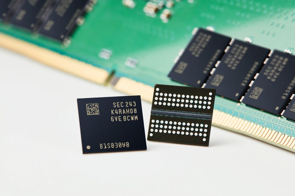
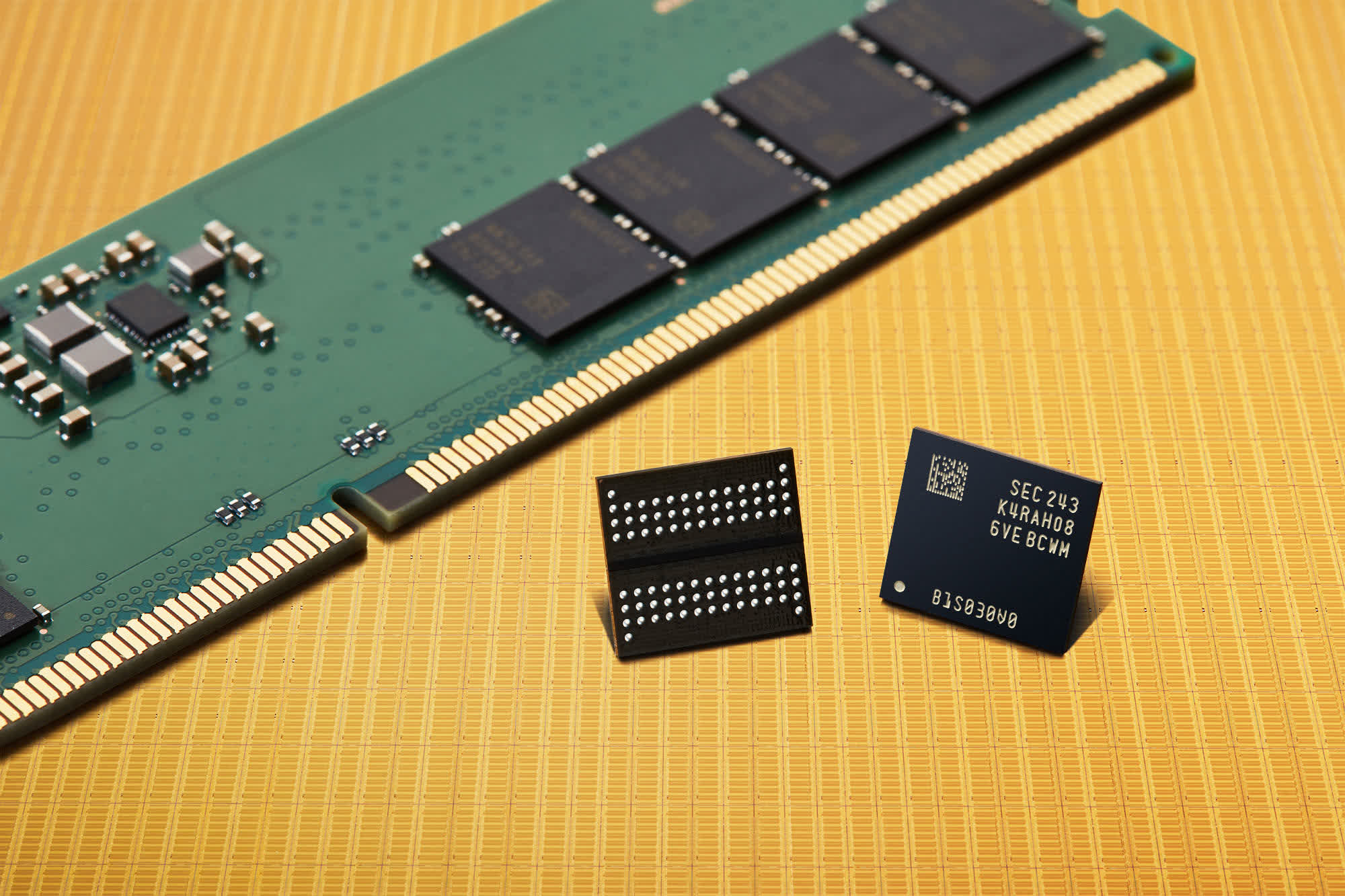
Working together with AMD, Samsung has completed the development of its 16-gigabit DDR5 DRAM chips, which will use the “industry’s first 12 nanometer-class process technology.” The Korean company describes these new chips as a leap that is”technological when it comes to business; AMD contributed to item analysis for compatibility with Zen-based CPUs.
Leveraging the latest DDR5 standard, Samsung describes, the newest potato chips will unlock speeds as high as 7.2 gigabits per 2nd (Gbps). This allows this new RAM segments to process two 30-gigabyte Ultra HD flicks in only one second.
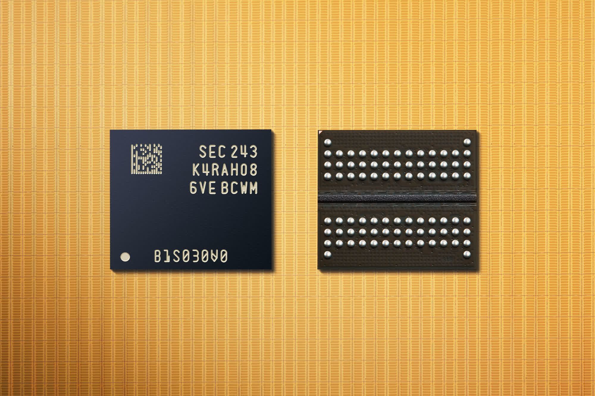
The 12nm potato chips tend to be produced having a multi-layer ultraviolet that is extremeEUV) lithography process, which is more expensive than deep ultraviolet (DUV) lithography machinery traditionally used for memory production. Samsung also used a new high-κ material that is dielectric increases cellular capacitance, as well as a proprietary design technology that gets better important circuit attributes.
The 12nm potato chips provide the business’s greatest perish thickness, allowing a 20 per cent gain in wafer output. The brand new DRAM chips are extremely quick and energy saving, ingesting as much as 23 % less energy than earlier DRAM services and products.
Samsung begins size creation of its 12nm DDR5 chips in 2023, with intends to broaden the organization’s DRAM lineup built in the technology that is new. The market segments Samsung is targeting include computing that is next-generation information facilities and AI-driven methods. Companies involved in those areas will have access to then faster performance while increasing sustainability and power efficiency.
Jooyoung Lee, Executive Vice President of DRAM Product & Technology at Samsung Electronics, said the company’s “12nm-range DRAM will be a key enabler in driving market-wide adoption of DDR5 DRAM.”
Joe Macri, Senior VP at AMD, highlighted how “innovation often requires close collaboration with industry partners to push the bounds of technology.” The new DDR5 chips will be optimized and validated on the* that is( system through the beginning, meaning the Santa Clara firm would like to maintain the advantage over rivals in giving support to the newest DDR5 requirements and rates.