[ad_1]
In a nutshell: Micron’s new 232-layer NAND has the very best TLC density within the trade at 14.6 Gb/mm2. It options improved storage capability, as much as 1Tb per die and 2TB per package deal. The firm can also be promoting over 75 % increased learn bandwidth and twice the write bandwidth of its past-gen 176-layer flash.
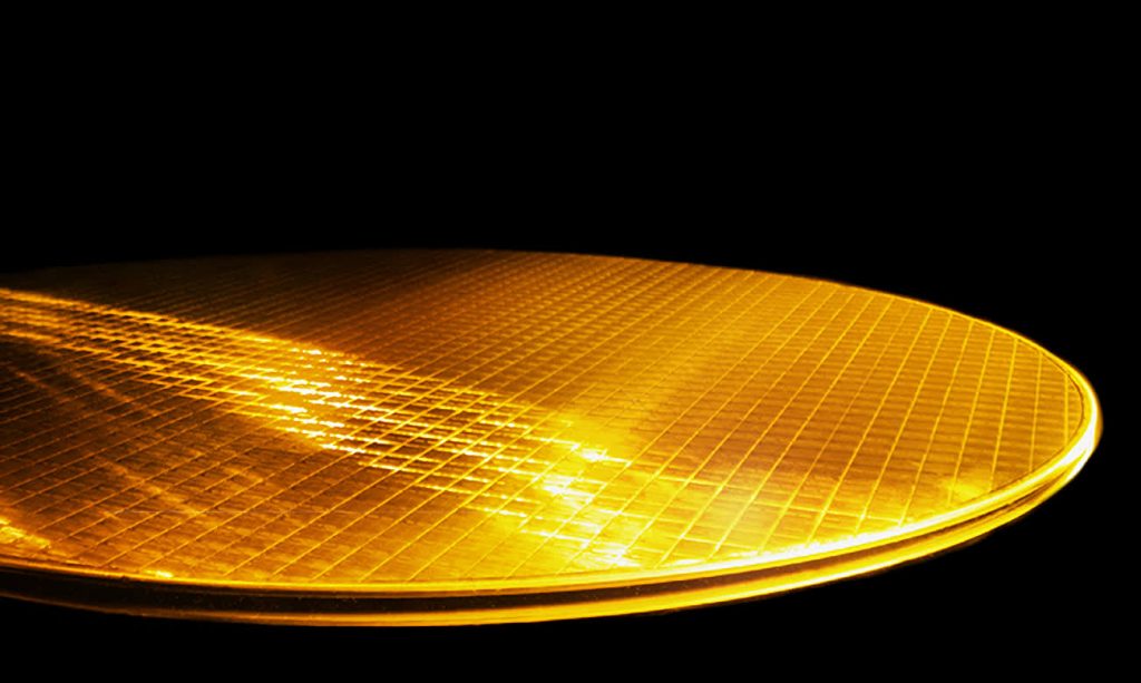
Micron introduced that it has began transport its 232-layer NAND to shoppers in element kind and thru its Crucial SSD client product line, regaining trade management in relation to layer rely.
The firm’s sixth era 3D NAND makes use of two 116-layer decks in a string-stacked design. It has a density of 14.6 Gbit/mm2, over 40 % increased than its earlier 176-layer flash. Micron additionally claims its areal density is 35 to 100% higher than competing TLC merchandise.
This elevated density allowed the corporate to shrink its chip packaging by 28 % in comparison with last-gen, right down to 11.5mm x 13.5mm. Micron’s new TLC flash has a die capability of 1Tb, that means it may well now produce 2TB packages when stacking 16 dies collectively.
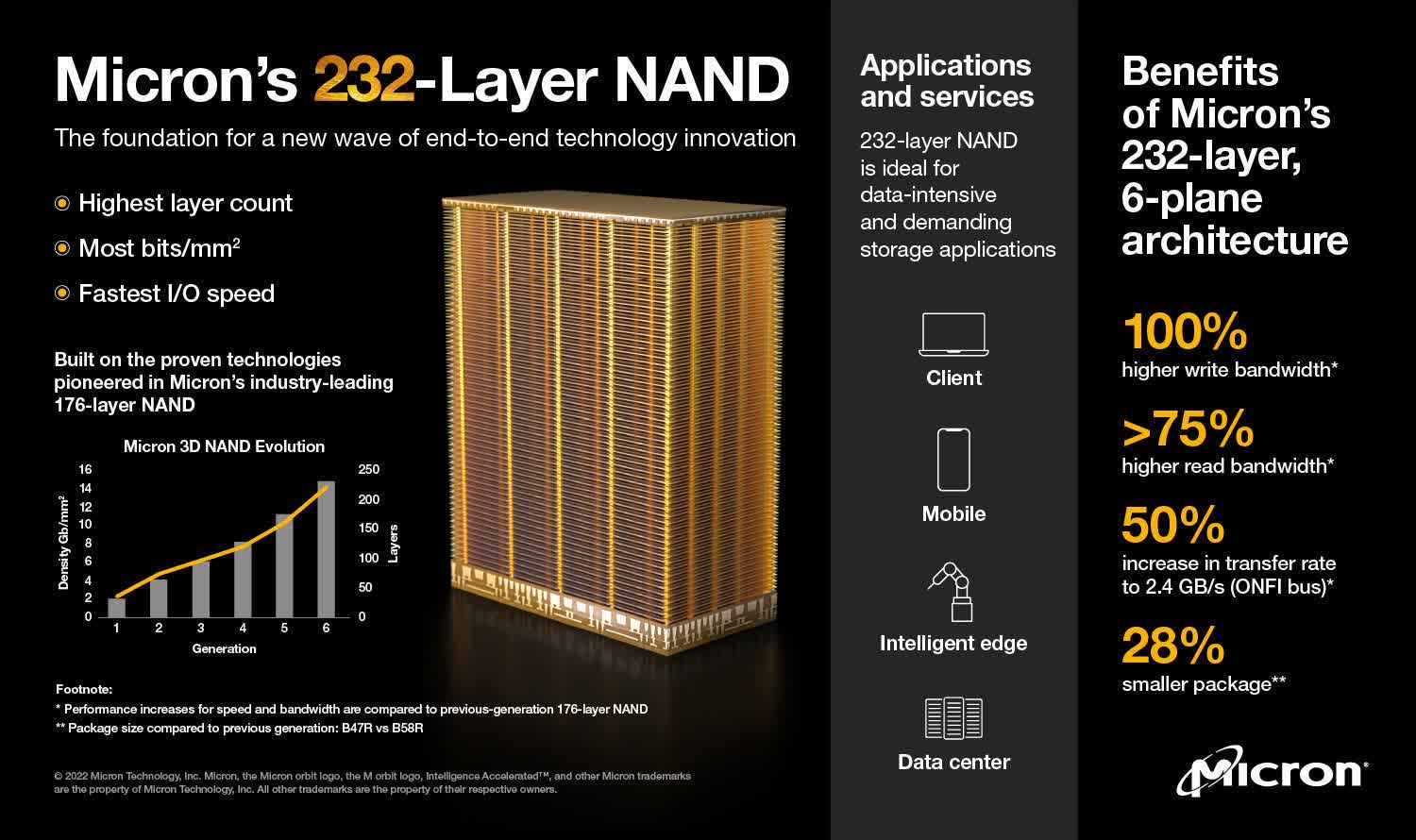
The new 232-layer NAND additionally options efficiency enhancements because it will increase the variety of planes per die from 4 to 6, enhancing parallelism. ONFi 5.0 will increase switch charges by 50 % to 2,400 MT/s whereas introducing a brand new NV-LPDDR4 interface that delivers per-bit power switch financial savings of over 30 %. Overall, Micron is touting over 75 % increased learn bandwidth, with write bandwidth doubling in comparison with previous-gen NAND.
Micron’s 232-layer NAND is presently in quantity manufacturing in its Singapore fab. The first SSDs geared up with it would most likely come to market in just a few months.
[ad_2]