In the world of GPUs, 2022 will go down as a milestone of their historical past. Intel made good on its promise of re-entering the discrete graphics card market, Nvidia pushed card sizes and costs by way of the roof, and AMD introduced CPU tech into the graphics enviornment. The information headlines ran replete with tales of disappointing efficiency, melting cables, and faked frames.
GPU fervor spilled into boards, with PC fans amazed and aghast in equal measure, as to what had grow to be of the graphics card market. So, it is simple to neglect that the most recent merchandise are housing probably the most advanced and highly effective chips which have ever graced a house pc.
Let’s deliver all of the distributors to the desk, and dive deep into their architectures, peeling away the layers to see what’s new, what they’ve in widespread, and simply what any of this implies to the common consumer. This is an extended article, with many sections, so use the next index to navigate by way of it. You may need to brush up on RDNA 2 and Ampere architectures earlier than you begin right here.
Article Index
Overall GPU Structure: Starting From the Top
Let’s begin with an necessary facet of this text — this isn’t a efficiency comparability. Instead, we’re taking a look at how the whole lot is organized inside a GPU, trying out the stats and figures to know the variations in strategy that AMD, Intel, and Nvidia have with regards to designing their graphics processors.
We’ll start with a have a look at the general GPU compositions for the most important chips accessible that use the architectures we’re inspecting. It’s necessary to emphasize that Intel’s providing is not focused on the identical market as AMD’s or Nvidia’s, as it is very a lot a mid-range graphics processor.
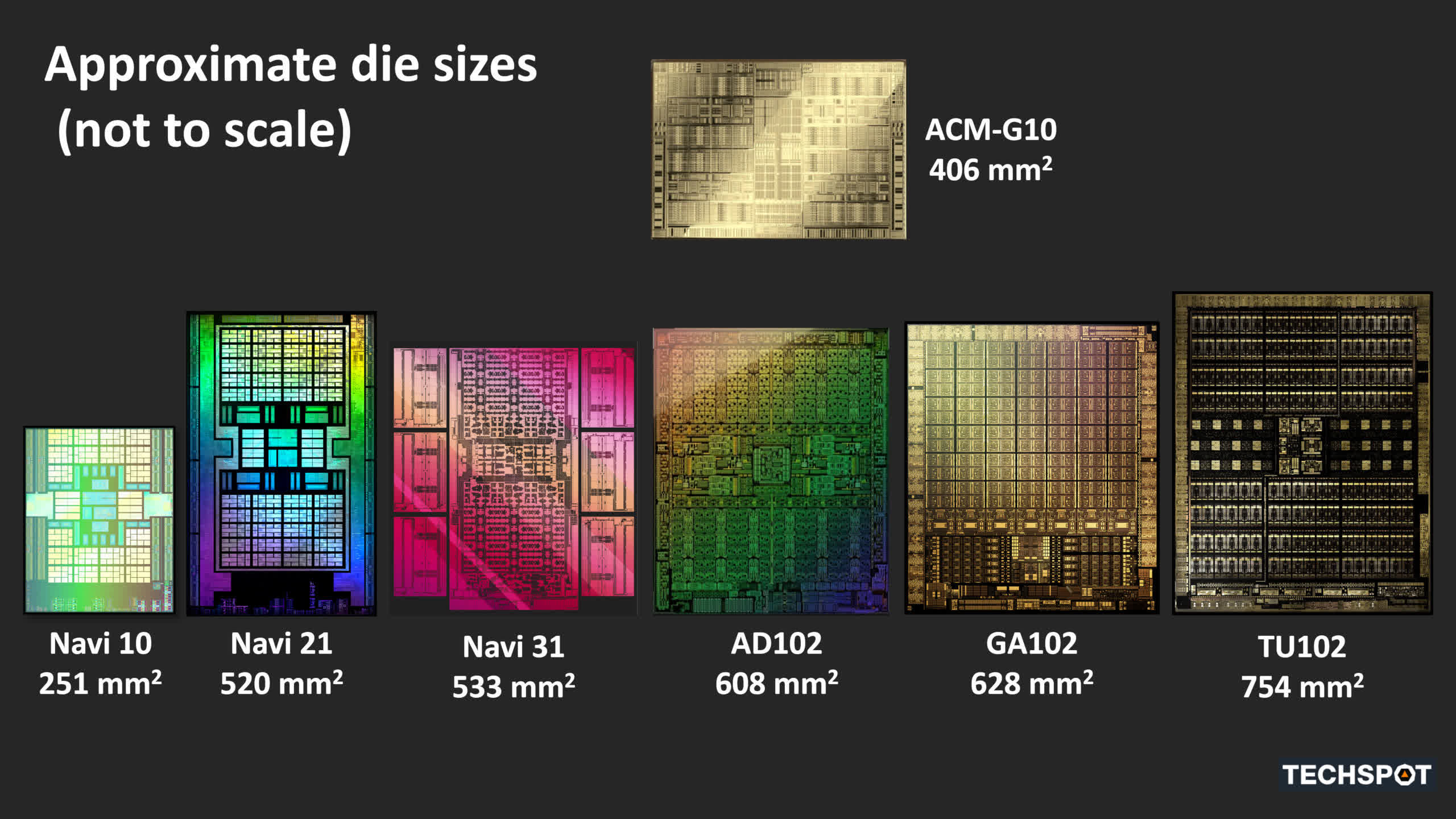
All three are fairly completely different in measurement, not solely to one another, but in addition to comparable chips utilizing earlier architectures. All of this evaluation is solely for understanding what precisely is underneath the hood in all three processors. We’ll look at the general constructions, earlier than breaking up the basic sections of every GPU — the shader cores, ray tracing skills, the reminiscence hierarchy, and the show and media engines.
AMD Navi 31
Taking issues alphabetically, the primary on the desk is AMD’s Navi 31, their largest RDNA 3-powered chip introduced up to now. Compared to the Navi 21, we will see a transparent development in element rely from their earlier top-end GPU…
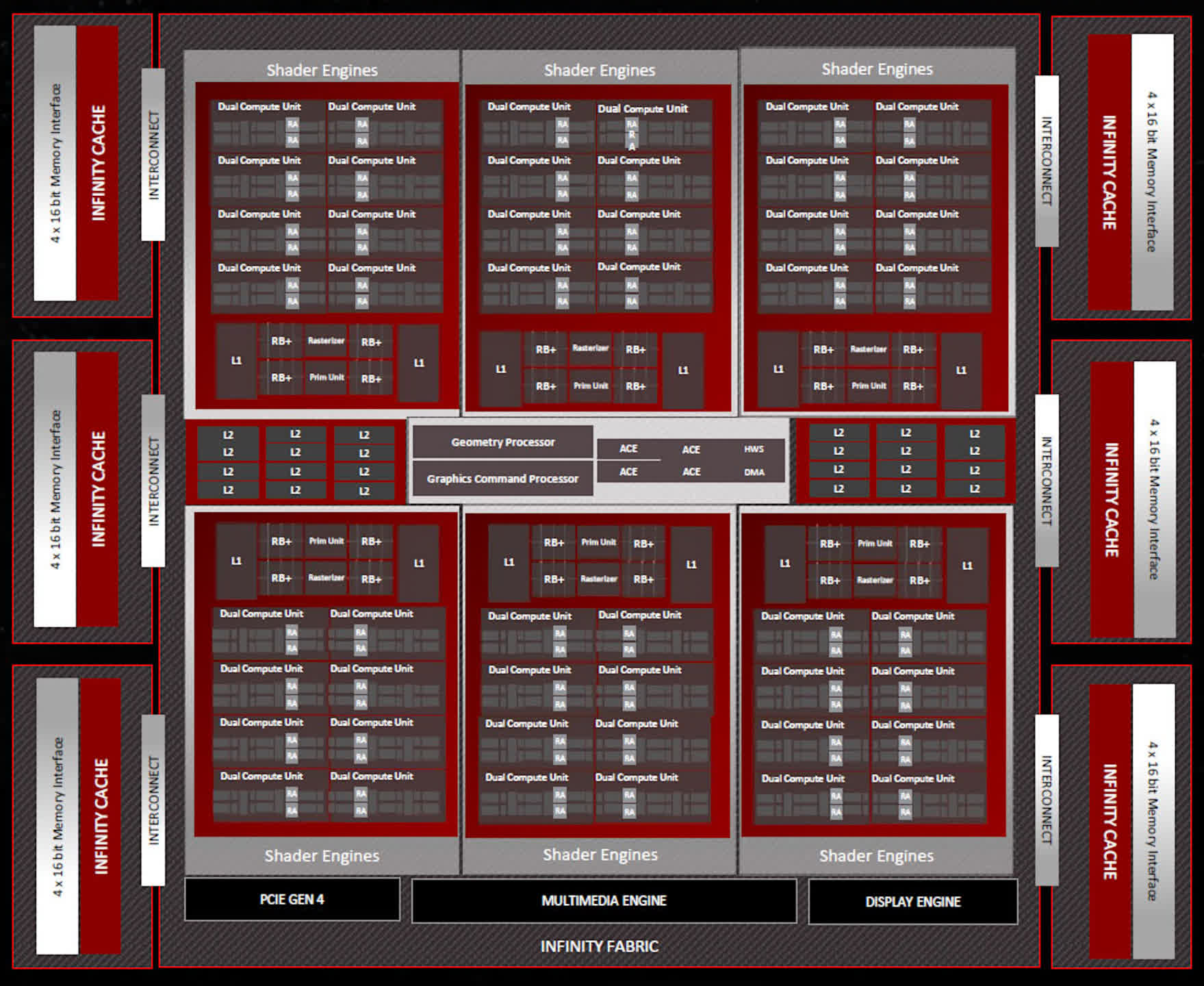
The Shader Engines (SE) home fewer Compute Units (CUs), 16 versus 200, however there at the moment are 6 SEs in complete — two greater than earlier than. This means Navi 31 has as much as 96 CUs, fielding a complete of 6144 Stream Processors (SP). AMD has accomplished a full improve of the SPs for RDNA 3 and we’ll sort out that later within the article.
Each Shader Engine additionally incorporates a devoted unit to deal with rasterization, a primitive engine for triangle setup, 32 render output items (ROPs), and two 256kB L1 caches. The final facet is now double the scale however the ROP rely per SE continues to be the identical.
AMD hasn’t modified the rasterizer and primitive engines a lot both — the said enhancements of fifty% are for the total die, because it has 50% extra SEs than the Navi 21 chip. However, there are adjustments to how the SEs deal with directions, similar to quicker processing of a number of draw instructions and higher administration of pipeline levels, which ought to cut back how lengthy a CU wants to attend earlier than it could possibly transfer on to a different job.
The most blatant change is the one which garnered probably the most rumors and gossip earlier than the November launch — the chiplet strategy to the GPU package deal. With a number of years of expertise on this area, it is considerably logical that AMD selected to do that, but it surely’s fully for value/manufacturing causes, somewhat than efficiency.

We’ll take a extra detailed have a look at this later within the article, so for now, let’s simply focus on what elements are the place. In the Navi 31, the reminiscence controllers and their related partitions of the final-tier cache are housed in separate chiplets (known as MCDs or Memory Cache Dies) that encompass the first processor (GCD, Graphics Compute Die).
With a larger variety of SEs to feed, AMD elevated the MC rely by 50%, too, so the whole bus width to the GDDR6 world reminiscence is now 384-bits. There’s much less Infinity Cache in complete this time (96MB vs 128MB), however the larger reminiscence bandwidth offsets this.
Intel ACM-G10
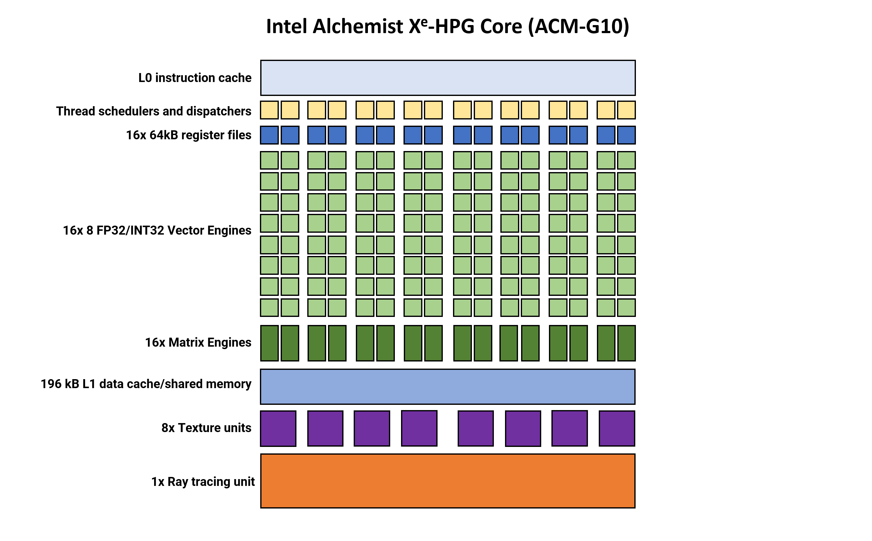
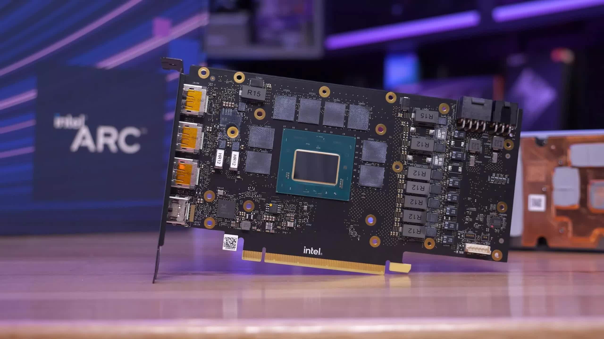
Onward to Intel and the ACM-G10 die (beforehand known as DG2-512). While this is not the most important GPU that Intel makes, it is their greatest client graphics die.
The block diagram is a reasonably commonplace association, although trying extra akin to Nvidia’s than AMD’s. With a complete of 8 Render Slices, every containing 4 Xe-Cores, for a complete rely of 512 Vector Engines (Intel’s equal of AMD’s Stream Processors and Nvidia’s CUDA cores).
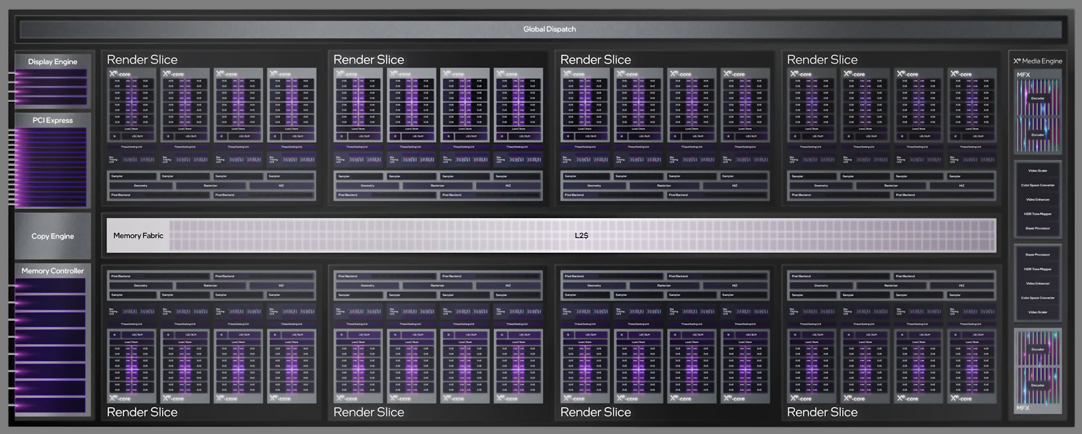
Also packed into every Render Slice is a primitive unit, rasterizer, depth buffer processor, 32 texture items, and 16 ROPs. At first look, this GPU would seem like fairly massive, as 256 TMUs and 128 ROPs are greater than that present in a Radeon RX 6800 or GeForce RTX 2080, for instance.
However, AMD’s RNDA 3 chip homes 96 Compute Units, every with 128 ALUs, whereas the ACM-G10’s sports activities a complete of 32 Xe Cores, with 128 ALUs per core. So, by way of ALU rely solely, Intel’s Alchemist-powered GPU is a 3rd the scale of AMD’s. But as we’ll see later, a major quantity of the ACM-G10’s die is given over to a unique number-crunching unit.
Compared to the primary Alchemist GPU that Intel launched through OEM suppliers, this chip has all of the hallmarks of a mature structure, by way of element rely and structural association.
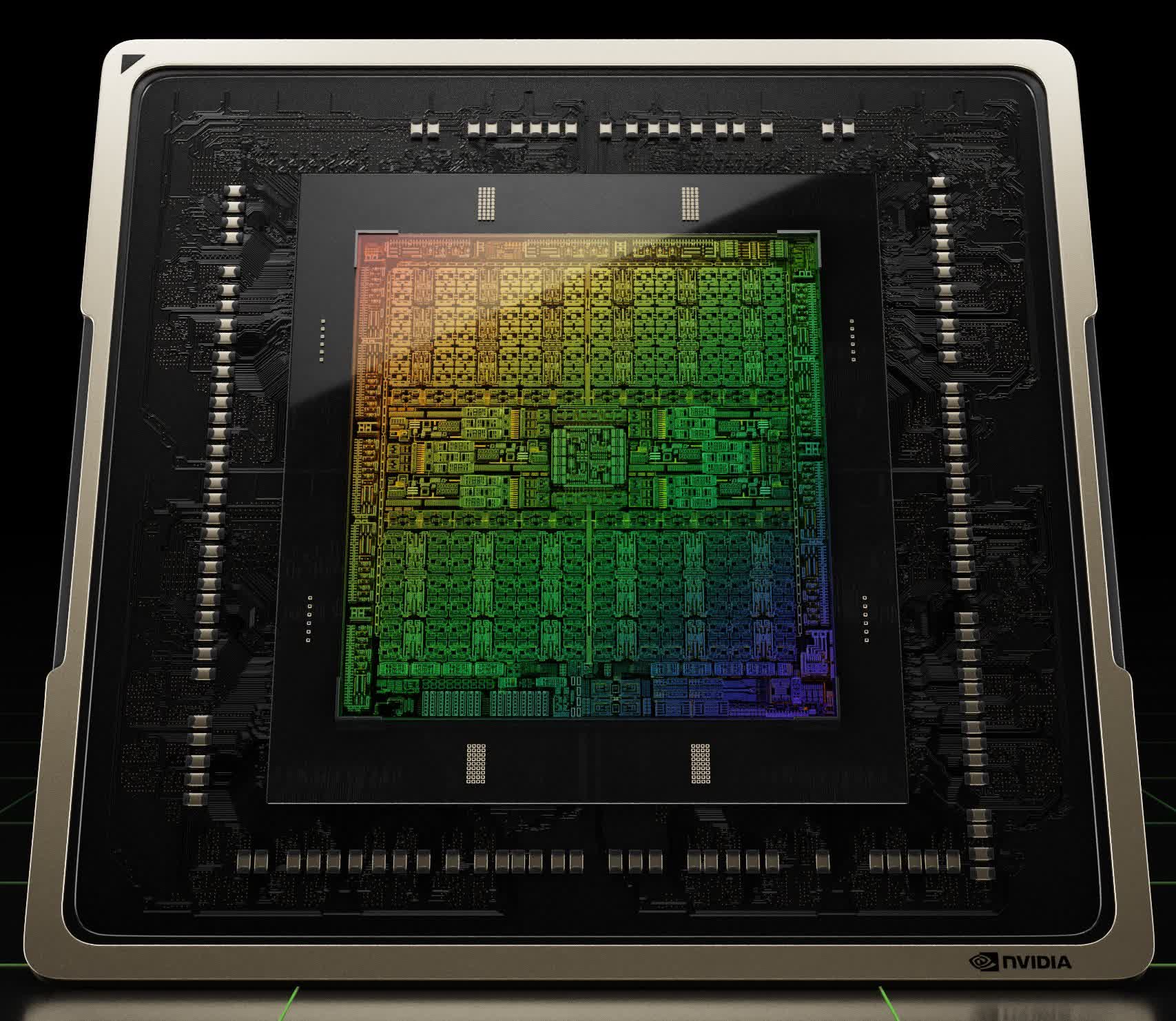
Nvidia AD102
We end our opening overview of the completely different layouts with Nvidia’s AD102, their first GPU to make use of the Ada Lovelace structure. Compared to its predecessor, the Ampere GA102, it would not appear all that completely different, only a lot bigger. And to all intents and functions, it’s.
Nvidia makes use of a element hierarchy of a Graphics Processing Cluster (GPU) that incorporates 6 Texture Processing Clusters (TPCs), with every of these housing 2 Streaming Multiprocessors (SMs). This association hasn’t modified with Ada, however the complete numbers actually have…
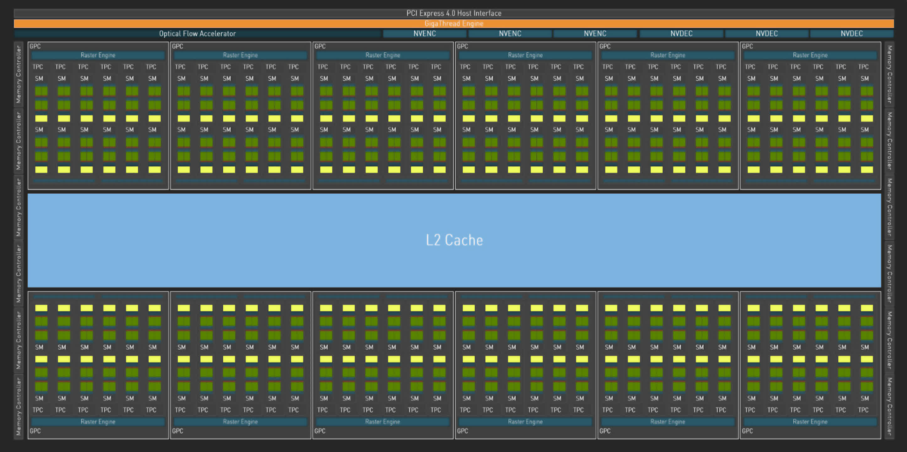
In the total AD102 die, the GPC rely has gone from 7 to 12, so there’s now a complete of 144 SMs, giving a complete of 18432 CUDA cores. This may appear to be a ridiculously excessive quantity when in comparison with the 6144 SPs in Navi 31, however AMD and Nvidia rely their parts otherwise.
Although that is grossly simplifying issues, one Nvidia SM is equal to 1 AMD CU — each comprise 128 ALUs. So the place Navi 31 is twice the scale of the Intel ACM-G10 (ALU rely solely), the AD102 is 3.5 instances bigger.
This is why it is unfair to do any outright efficiency comparisons of the chips once they’re so clearly completely different by way of scale. However, as soon as they’re inside a graphics card, priced and marketed, then it is a completely different story.
But what we will examine are the smallest repeated elements of the three processors.
Shader Cores: Into the Brains of the GPU
From the overview of the entire processor, let’s now dive into the hearts of the chips, and have a look at the basic number-crunching elements of the processors: the shader cores.
The three producers use completely different phrases and phrases with regards to describing their chips, particularly with regards to their overview diagrams. So for this text, we will use our personal photographs, with widespread colours and constructions, in order that it is simpler to see what’s the identical and what’s completely different.
AMD RDNA 3
AMD’s smallest unified construction inside the shading a part of the GPU is known as a Double Compute Unit (DCU). In some paperwork, it is nonetheless known as a Workgroup Processor (WGP), whereas others confer with it as a Compute Unit Pair.
Please observe that if one thing is not proven in these diagrams (e.g. constants caches, double precision items) that does not imply they are not current within the structure.
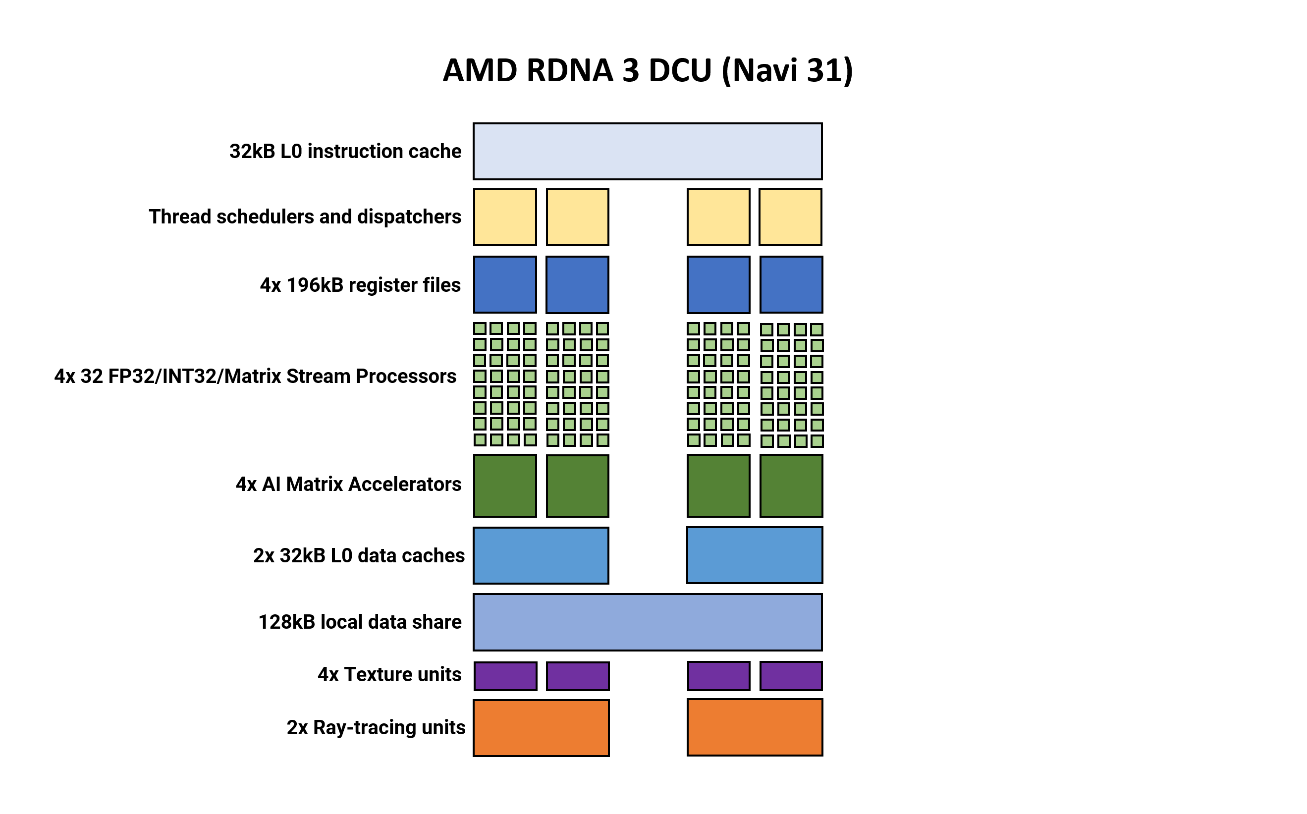
In some ways, the general format and structural parts have not modified a lot from RDNA 2. Two Compute Units share some caches and reminiscence, and every one includes two units of 32 Stream Processors (SP).
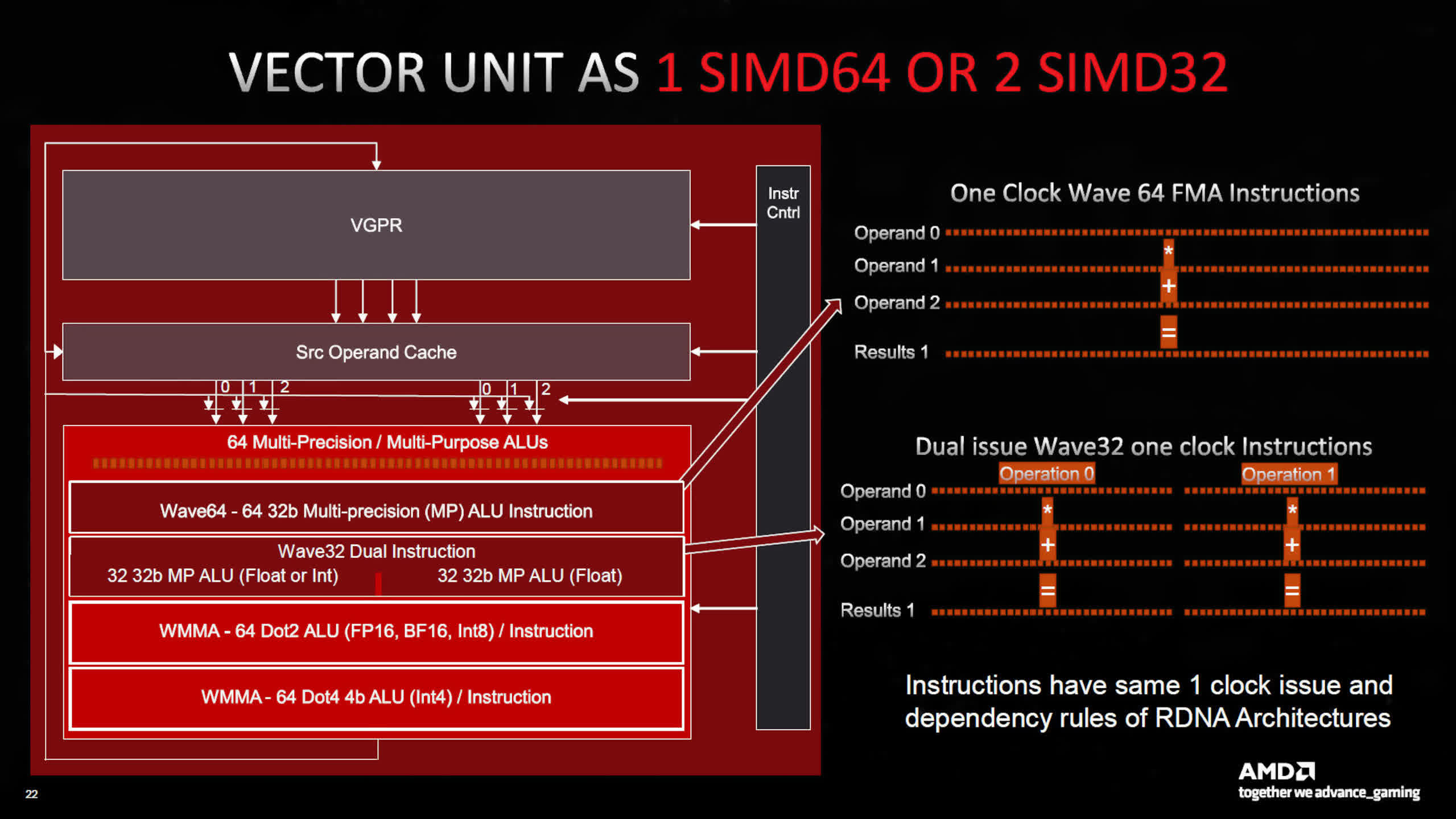
What’s new for model 3, is that every SP now homes twice as many arithmetic logic items (ALUs) as earlier than. There at the moment are two banks of SIMD64 items per CU and every financial institution has two dataports — one for floating level, integer, and matrix operations, with the opposite for simply float and matrix.
AMD does use separate SPs for various knowledge codecs — the Compute Units in RDNA 3 helps operation utilizing FP16, BF16, FP32, FP64, INT4, INT8, INT16, and INT32 values.
The use of SIMD64 signifies that every thread scheduler can ship out a gaggle of 64 threads (known as a wavefront), or it could possibly co-issue two wavefronts of 32 threads, per clock cycle. AMD has retained the identical instruction guidelines from earlier RDNA architectures, so that is one thing that is dealt with by the GPU/drivers.
Another vital new function is the looks of what AMD calls AI Matrix Accelerators.
Unlike Intel’s and Nvidia’s structure, which we’ll see shortly, these do not act as separate items — all matrix operations make the most of the SIMD items and any such calculations (known as Wave Matrix Multiply Accumulate, WMMA) will use the total financial institution of 64 ALUs.
At the time of writing, the precise nature of the AI Accelerators is not clear, but it surely’s most likely simply circuitry related to dealing with the directions and the massive quantity of information concerned, to make sure most throughput. It could effectively have the same operate to that of Nvidia’s Tensor Memory Accelerator, of their Hopper structure.
Compared to RDNA 2, the adjustments are comparatively small — the older structure might additionally deal with 64 thread wavefronts (aka Wave64), however these had been issued over two cycles and used each SIMD32 blocks in every Compute Unit. Now, this may all be accomplished in a single cycle and can solely use one SIMD block.
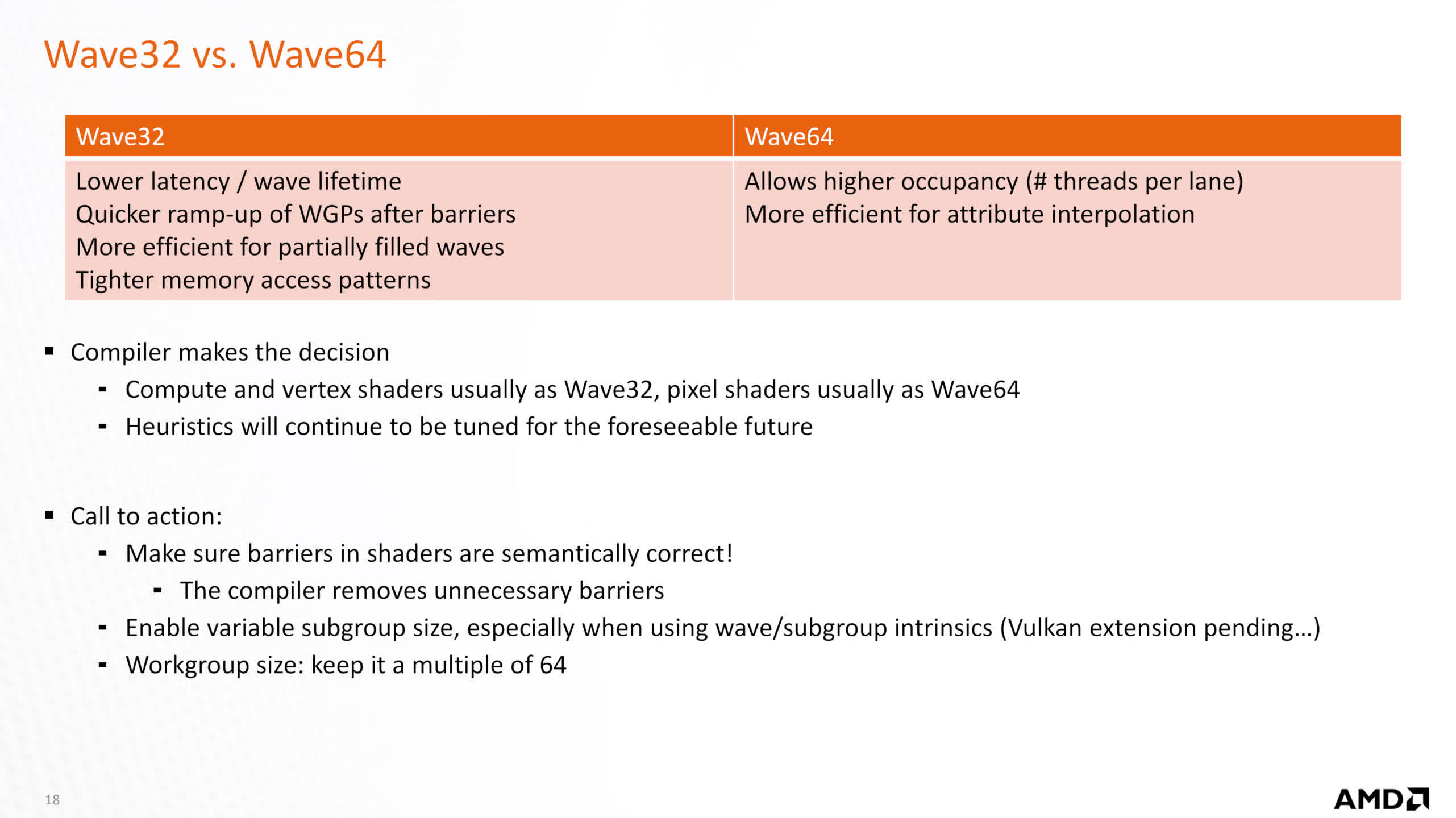
In earlier documentation, AMD said that Wave32 was usually used for compute and vertex shaders (and possibly ray shaders, too), whereas Wave 64 was largely for pixel shaders, with the drivers compiling shaders accordingly. So the transfer to single cycle Wave64 instruction subject will present a lift to video games which are closely depending on pixel shaders.
However, all of this additional energy on faucet must be appropriately utilized as a way to take full benefit of it. This is one thing that is true of all GPU architectures and so they all should be closely loaded with a number of threads, as a way to do that (it additionally helps conceal the inherent latency that is related to DRAM).
So with doubling the ALUs, AMD has pushed the necessity for programmers to make use of instruction-level parallelism as a lot as attainable. This is not one thing new on this planet of graphics, however one vital benefit that RDNA had over AMD’s previous GCN structure was that it did not want as many threads in flight to succeed in full utilization. Given how advanced trendy rendering has grow to be in video games, builders are going to have a little bit extra work on their palms, with regards to writing their shader code.
Intel Alchemist
Let’s transfer on to Intel now, and have a look at the DCU-equivalent within the Alchemist structure, known as an Xe Core (which we’ll abbreviate to XEC). At first look, these look completely big compared to AMD’s construction.
Where a single DCU in RDNA 3 homes 4 SIMD64 blocks, Intel’s XEC incorporates sixteen SIMD8 items, every one managed by its personal thread scheduler and dispatch system. Like AMD’s Streaming Processors, the so-called Vector Engines in Alchemist can deal with integer and float knowledge codecs. There’s no help for FP64, however this is not a lot of a problem in gaming.
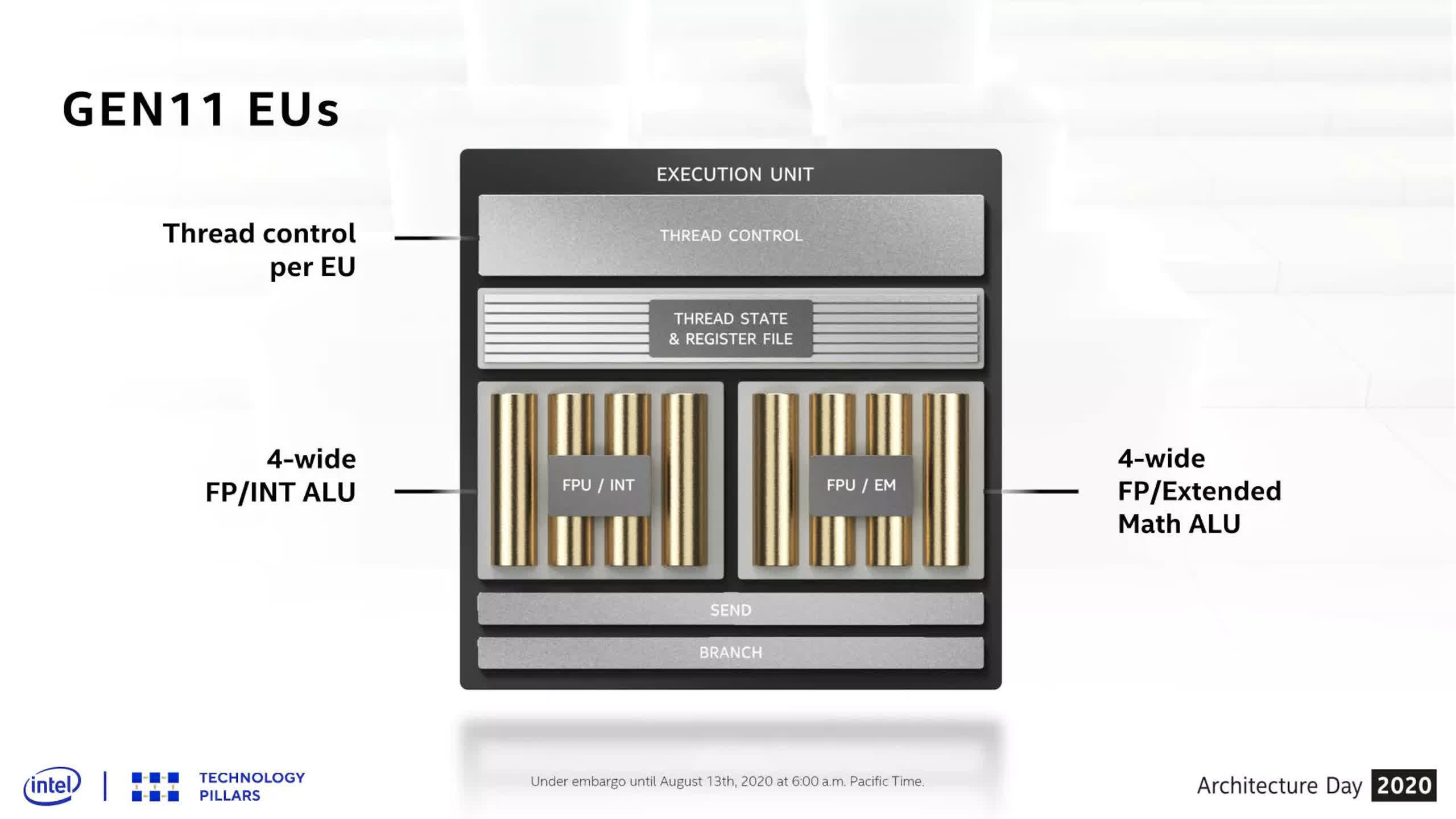
Intel has at all times used comparatively slim SIMDs — these utilized in likes of Gen11 had been solely 4-wide (i.e. deal with 4 threads concurrently) and solely doubled in width with Gen 12 (as used of their Rocket Lake CPUs, for instance).
But provided that the gaming trade has been used to SIMD32 GPUs for an excellent variety of years, and thus video games are coded accordingly, the choice to maintain the slim execution blocks appears counter-productive.
Where AMD’s RDNA 3 and Nvidia’s Ada Lovelace have processing blocks that may be issued 64 or 32 threads in a single cycle, Intel’s structure requires 4 cycles to realize the identical end result on one VE — therefore why there are sixteen SIMD items per XEC.
However, which means that if video games aren’t coded in such a approach to make sure the VEs are absolutely occupied, the SIMDs and related sources (cache, bandwidth, and so on.) will likely be left idle. A standard theme in benchmark outcomes with Intel’s Arc-series of graphics playing cards is that they have a tendency to do higher at greater resolutions and/or in video games with a number of advanced, trendy shader routines.
This is partly as a result of excessive stage of unit subdivision and useful resource sharing that takes place. Micro-benchmarking evaluation by web site Chips and Cheese reveals that for all its wealth of ALUs, the structure struggles to realize correct utilization.
Moving on to different elements within the XEC, it isn’t clear how massive the Level 0 instruction cache is however the place AMD’s are 4-way (as a result of it serves 4 SIMD blocks), Intel’s should be 16-way, which provides to the complexity of the cache system.
Intel additionally selected to supply the processor with devoted items for matrix operations, one for every Vector Engine. Having this many items means a good portion of the die is devoted to dealing with matrix math.
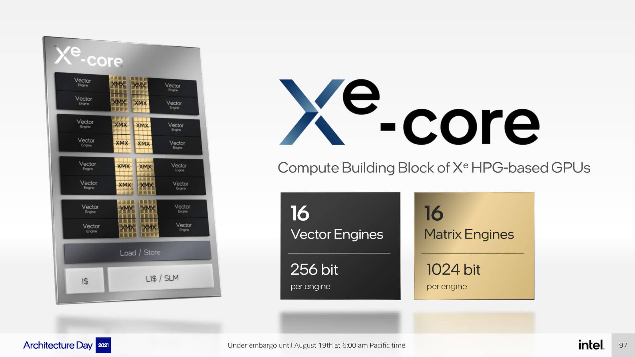
Where AMD makes use of the DCU’s SIMD items to do that and Nvidia has 4 comparatively massive tensor/matrix items per SM, Intel’s strategy appears a little bit extreme, provided that they’ve a separate structure, known as Xe-HP, for compute functions.
Another odd design appears to be the load/retailer (LD/ST) items within the processing block. Not proven in our diagrams, these handle reminiscence directions from threads, transferring knowledge between the register file and the L1 cache. Ada Lovelace is similar to Ampere with 4 per SM partition, giving 16 in complete. RDNA 3 can be the identical as its predecessor, with every CU having devoted LD/ST circuitry as a part of the feel unit.
Intel’s Xe-HPG presentation reveals only one LD/ST per XEC however in actuality, it is most likely composed of additional discrete items inside. However, of their optimization information for OneAPI, a diagram means that the LD/ST cycles by way of the person register information one by one. If that is the case, then Alchemist will at all times battle to realize most cache bandwidth effectivity, as a result of not all information are being served on the identical time.
Nvidia Ada Lovelace
The final processing block to take a look at is Nvidia’s Streaming Multiprocessor (SM) — the GeForce model of the DCU/XEC. This construction hasn’t modified an ideal deal from the 2018 Turing structure. In reality, it is virtually similar to Ampere.
Some of the items have been tweaked to enhance their efficiency or function set, however for probably the most half, there’s not an ideal deal that is new to speak about. Actually, there might be, however Nvidia is notoriously shy at revealing a lot concerning the internal operations and specs of their chips. Intel offers a little bit extra element, however the info is usually buried in different paperwork.
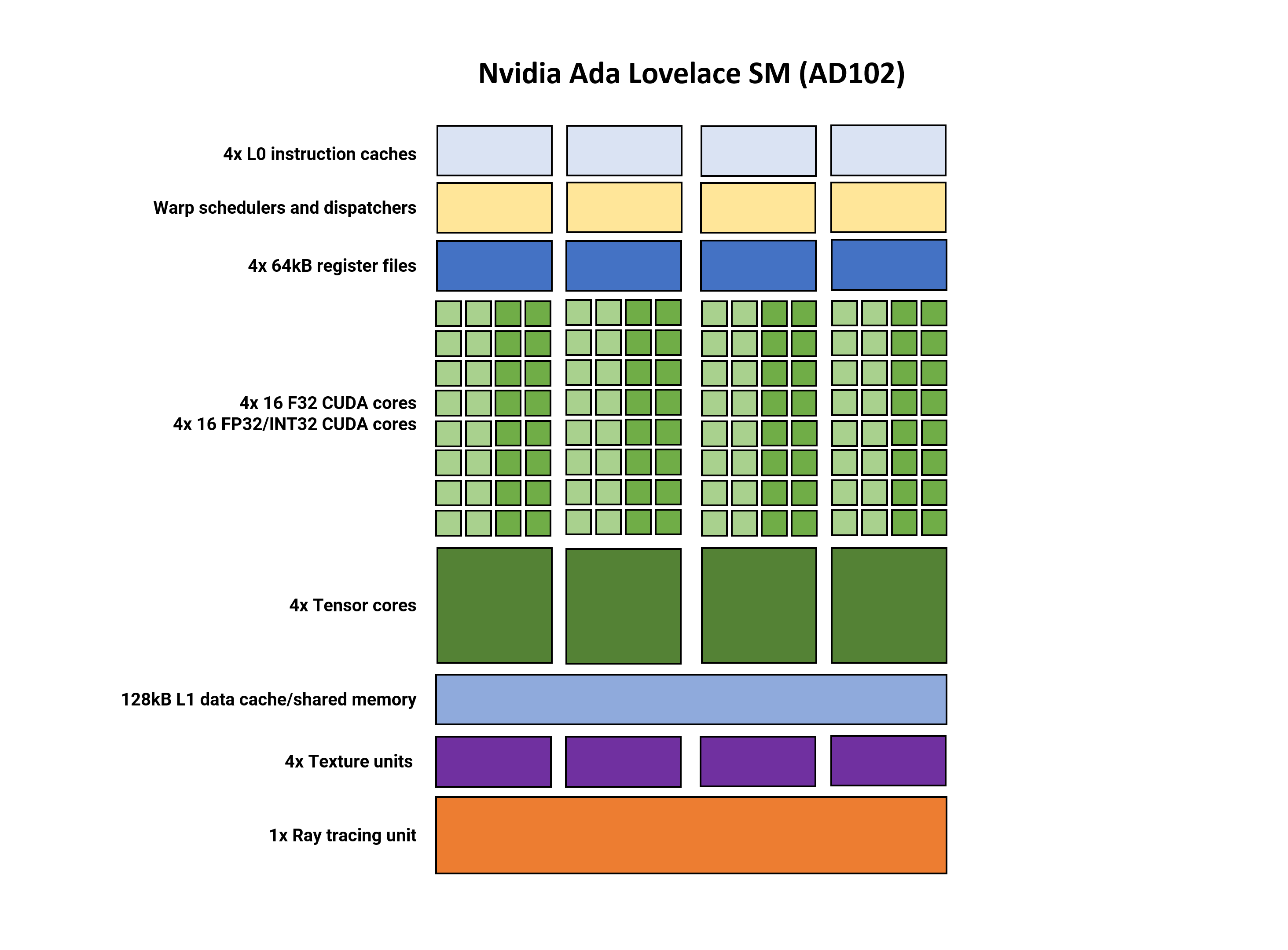
But to summarize the construction, the SM is break up into 4 partitions. Each one has its personal L0 instruction cache, thread scheduler and dispatch unit, and a 64 kB part of the register file paired to a SIMD32 processor.
Just as in AMD’s RDNA 3, the SM helps dual-issued directions, the place every partition can concurrently course of two threads, one with FP32 directions and the opposite with FP32 or INT32 directions.
Nvidia’s Tensor cores at the moment are of their 4th revision however this time, the one notable change was the inclusion of the FP8 Transformer Engine from their Hopper chip — uncooked throughput figures stay unaltered.
The addition of the low-precision float format signifies that the GPU ought to be extra appropriate for AI coaching fashions. The Tensor cores nonetheless additionally supply the sparsity function from Ampere, which may present as much as double the throughput.
Another enchancment lies within the Optical Flow Accelerator (OFA) engine (not proven in our diagrams). This circuit generates an optical movement area, which is used as a part of the DLSS algorithm. With double the efficiency of the OFA in Ampere, the additional throughput is utilized within the newest model of their temporal, anti-aliasing upscaler, DLSS 3.
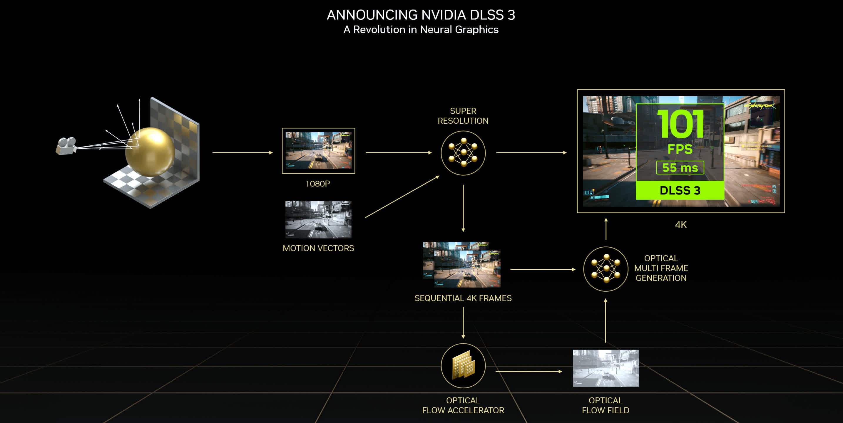
DLSS 3 has already confronted a good quantity of criticism, centering round two elements: the DLSS-generated frames aren’t ‘actual’ and the method provides extra latency to the rendering chain. The first is not fully invalid, because the system works by first having the GPU render two consecutive frames, storing them in reminiscence, earlier than utilizing a neural community algorithm to find out what an middleman body would seem like.
The current chain then returns to the primary rendered body and shows that one, adopted by the DLSS-frame, after which the second body rendered. Because the sport’s engine hasn’t cycled for the center body, the display screen is being refreshed with none potential enter. And as a result of the 2 successive frames should be stalled, somewhat than introduced, any enter that has been polled for these frames may even get stalled.
Whether DLSS 3 ever turns into standard or commonplace stays to be seen.
Although the SM of Ada is similar to Ampere, there are notable adjustments to the RT core and we’ll deal with these shortly. For now, let’s summarize the computational capabilities of AMD, Intel, and Nvidia’s GPU repeated constructions.
Processing Block Comparison
We can examine the SM, XEC, and DCU capabilities by trying on the variety of operations, for normal knowledge codecs, per clock cycle. Note that these are peak figures and are usually not essentially achievable in actuality.
| Operations per clock | Ada Lovelace | Alchemist | RDNA 3 |
| FP32 | 128 | 128 | 256 |
| FP16 | 128 | 256 | 512 |
| FP64 | 2 | n/a | 16 |
| INT32 | 64 | 128 | 128 |
| FP16 matrix | 512 | 2048 | 256 |
| INT8 matrix | 1024 | 4096 | 256 |
| INT4 matrix | 2048 | 8192 | 1024 |
Nvidia’s figures have not modified from Ampere, whereas RDNA 3’s numbers have doubled in some areas. Alchemist, although, is on one other stage with regards to matrix operations, though the truth that these are peak theoretical values ought to be emphasised once more.
Given that Intel’s graphics division leans closely in the direction of knowledge middle and compute, identical to Nvidia does, it isn’t shocking to see the structure dedicate a lot die area to matrix operations. The lack of FP64 functionality is not an issue, as that knowledge format is not actually utilized in gaming, and the performance is current of their Xe-HP structure.
Ada Lovelace and Alchemist are, theoretically, stronger than RDNA 3 with regards to matrix/tensor operations, however since we’re taking a look at GPUs which are primarily used for gaming workloads, the devoted items largely simply present acceleration for algorithms concerned in DLSS and XeSS — these use a convolutional auto-encoder neural community (CAENN) that scans a picture for artifacts and corrects them.
AMD’s temporal upscaler (FidelityFX Super Resolution, FSR) would not use a CAENN, because it’s based mostly totally on a Lanczos resampling technique, adopted by various picture correction routines, processed through the DCUs. However, within the RDNA 3 launch, the subsequent model of FSR was briefly launched, citing a brand new function known as Fluid Motion Frames. With a efficiency uplift of as much as double that of FSR 2.0, the overall consensus is that that is more likely to contain body era, as in DLSS 3, however whether or not this includes any matrix operations is but to be clear.
Ray Tracing for Everybody Now
With the launch of their Arc graphics playing cards sequence, utilizing the Alchemist structure, Intel joined AMD and Nvidia in providing GPUs that supplied devoted accelerators for numerous algorithms concerned with the usage of ray tracing in graphics. Both Ada and RNDA 3 comprise considerably up to date RT items, so it is smart to check out what’s new and completely different.
Starting with AMD, the largest change to their Ray Accelerators is including {hardware} to enhance the traversal of the bounding quantity hierarchies (BVH). These are knowledge constructions which are used to hurry up figuring out what floor a ray of sunshine has hit, within the 3D world.
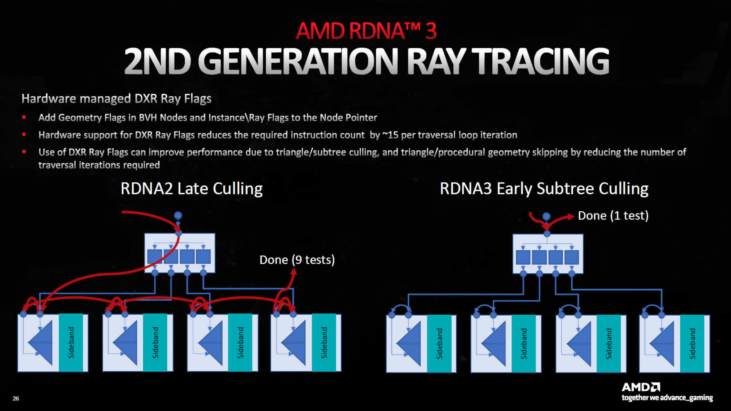
In RDNA 2, all of this work was processed through the Compute Units, and to a sure extent, it nonetheless is. However, for DXR, Microsoft’s ray tracing API, there’s {hardware} help for the administration of ray flags.
The use of those can tremendously cut back the variety of instances the BVH must be traversed, lowering the general load on cache bandwidth and compute items. In essence, AMD has centered on enhancing the general effectivity of the system they launched within the earlier structure.
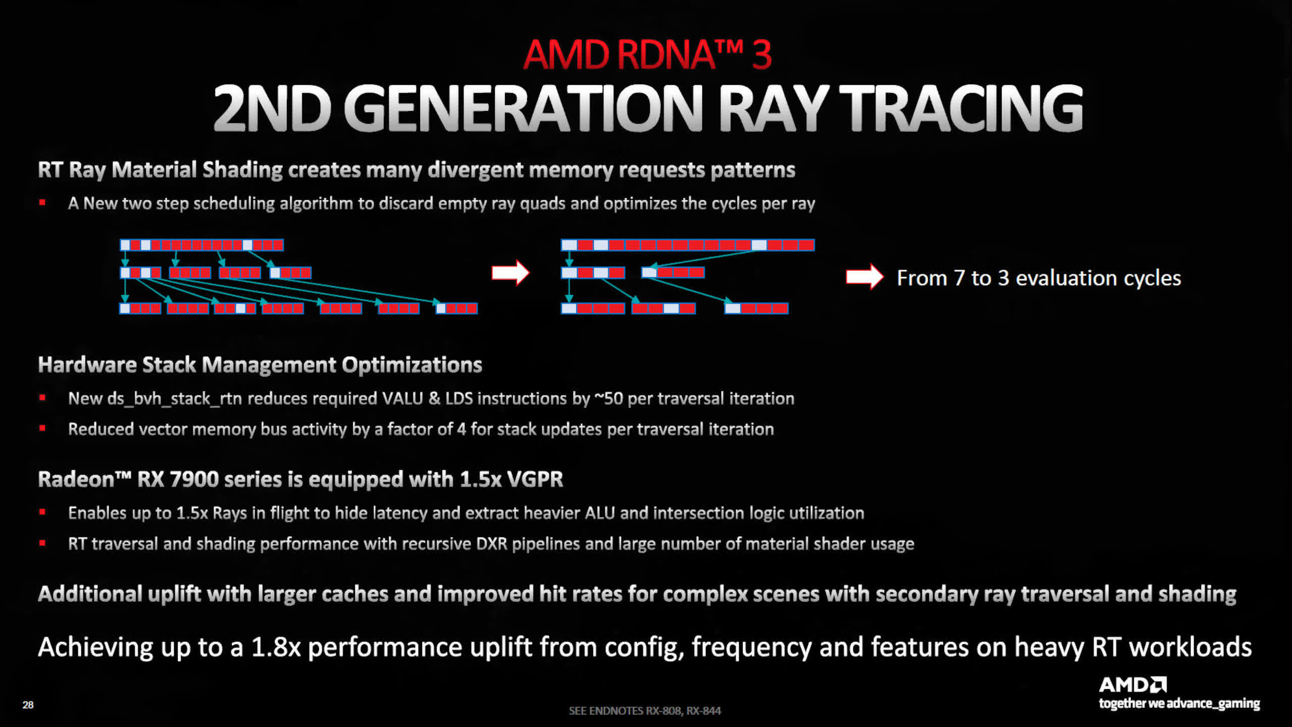
Additionally, the {hardware} has been up to date to enhance field sorting (which makes traversal quicker) and culling algorithms (to skip testing empty bins). Coupled with enhancements to the cache system, AMD states that there is as much as 80% extra ray tracing efficiency, on the identical clock velocity, in comparison with RDNA 2.
However, such enhancements don’t translate into 80% extra frames per second in video games utilizing ray tracing — the efficiency in these conditions is ruled by many components and the capabilities of the RT items is only one of them.
With Intel being new to the ray tracing recreation, there are not any enhancements as such. Instead, we’re merely instructed that their RT items deal with BVH traversal and intersection calculations, between rays and triangles. This makes them extra akin to Nvidia’s system than AMD’s, however there’s not a substantial amount of info accessible about them.
But we do know that every RT unit has an unspecified-sized cache for storing BVH knowledge and a separate unit for analyzing and sorting ray shader threads, to enhance SIMD utilization.
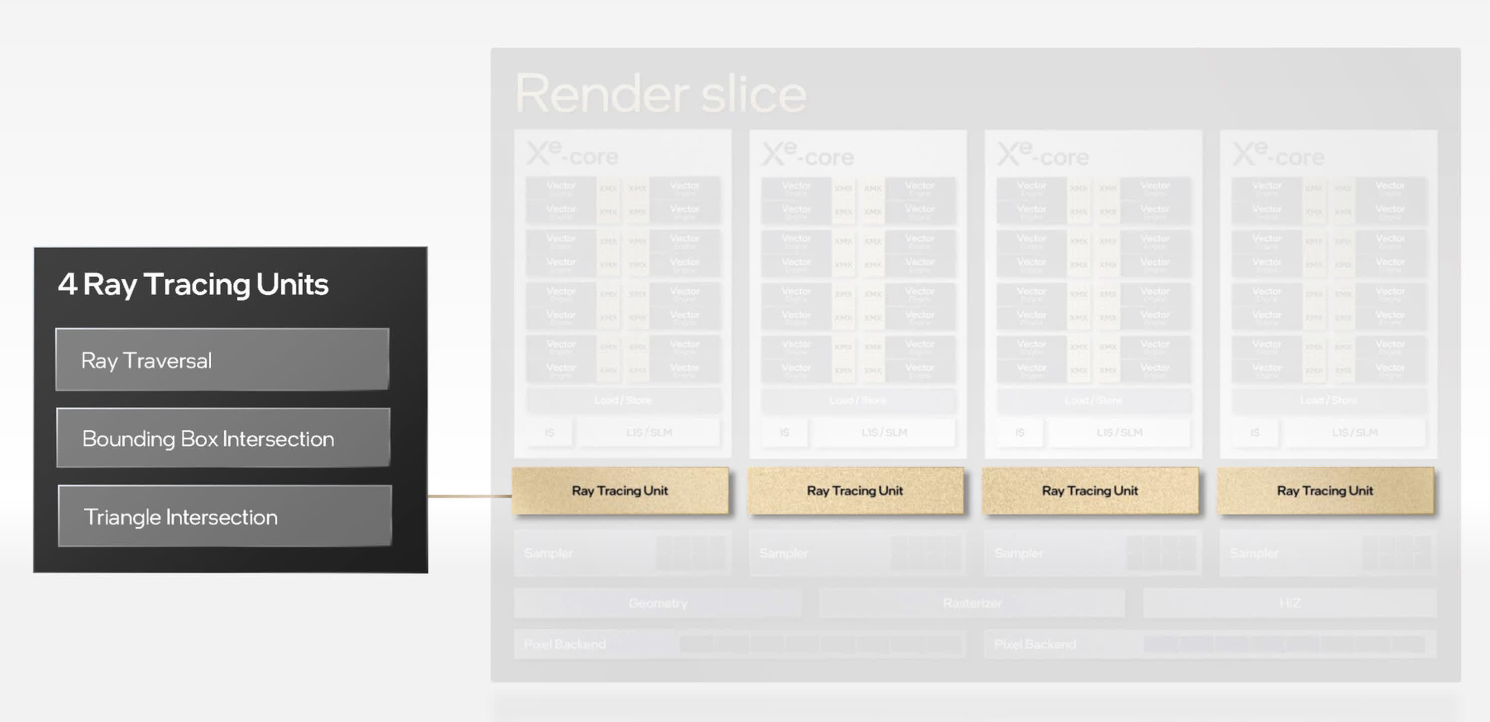
Each XEC is paired with one RT unit, giving a complete of 4 per Render Slice. Some early testing of the A770 with ray tracing enabled in video games reveals that no matter constructions Intel has in place, Alchemist’s general functionality in ray tracing is no less than pretty much as good as that discovered with Ampere chips, and a little bit higher than RDNA 2 fashions.
But allow us to repeat once more that ray tracing additionally locations heavy stress on the shading cores, cache system, and reminiscence bandwidth, so it isn’t attainable to extract the RT unit efficiency from such benchmarks.
For the Ada Lovelace structure, Nvidia made various adjustments, with suitably massive claims for the efficiency uplift, in comparison with Ampere. The accelerators for ray-triangle intersection calculations are claimed to have double the throughput, and BVH traversal for non-opaque surfaces is now mentioned to be twice as quick. The latter is necessary for objects that use textures with an alpha channel (transparency), for instance, leaves on a tree.
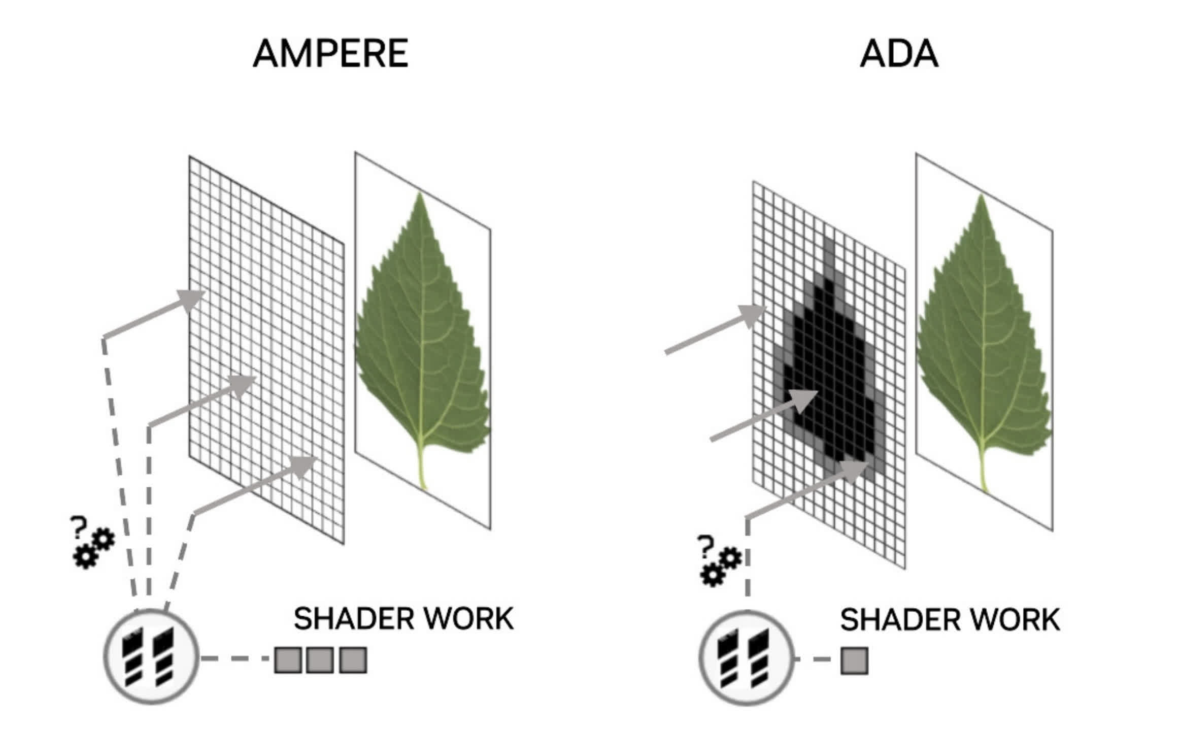
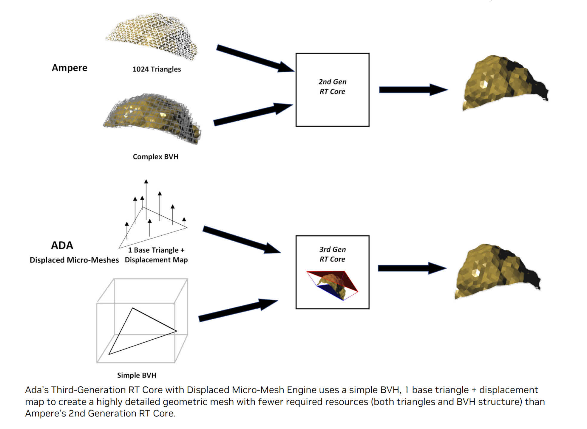
A ray hitting a completely clear part of such a floor should not end in a success end result — the ray ought to move straight by way of. However, to precisely decide this in present video games with ray tracing, a number of different shaders should be processed. Nvidia’s new Opacity Micromap Engine breaks up these surfaces into additional triangles after which determines what precisely is occurring, lowering the variety of ray shaders required.
Two additional additions to the ray tracing skills of Ada are a discount in construct time and reminiscence footprint of the BVHs (with claims of 10x quicker and 20x smaller, respectively), and a construction to reorder threads for ray shaders, giving higher effectivity. However, the place the previous requires no adjustments in software program by builders, the latter is at present solely accessed by an API from Nvidia, so it is of no profit to present DirectX 12 video games.
When we examined the GeForce RTX 4090’s ray tracing efficiency, the common drop in body fee with ray tracing enabled, was slightly below 45%. With the Ampere-powered GeForce RTX 3090 Ti, the drop was 56%. However, this enchancment can’t be solely attributed to the RT core enhancements, because the 4090 has considerably extra shading throughput and cache than the earlier mannequin.
We’ve but to see how what sort of distinction RDNA 3’s ray tracing enhancements quantity to, but it surely’s price noting that not one of the GPU producers expects RT for use in isolation — i.e. the usage of upscaling continues to be required to realize excessive body charges.
Fans of ray tracing could also be considerably dissatisfied that there have not been any main beneficial properties on this space, with the brand new spherical of graphics processors, however lots of progress has been created from when it first appeared, again in 2018 with Nvidia’s Turing structure.
Memory: Driving Down the Data Highways
GPUs crunch by way of knowledge like no different chip and preserving the ALUs fed with numbers is essential to their efficiency. In the early days of PC graphics processors, there was barely any cache inside and the worldwide reminiscence (the RAM utilized by all the chip) was desperately sluggish DRAM. Even simply 10 years in the past, the scenario wasn’t that significantly better.
So let’s dive into what is the present state of affairs, beginning with AMD’s reminiscence hierarchy of their new structure. Since its first iteration, RDNA has used a posh, multi-level reminiscence hierarchy. The greatest adjustments got here final yr when an enormous quantity of L3 cache was added to the GPU, as much as 128MB in sure fashions.
This continues to be the case for spherical three, however with some refined adjustments.
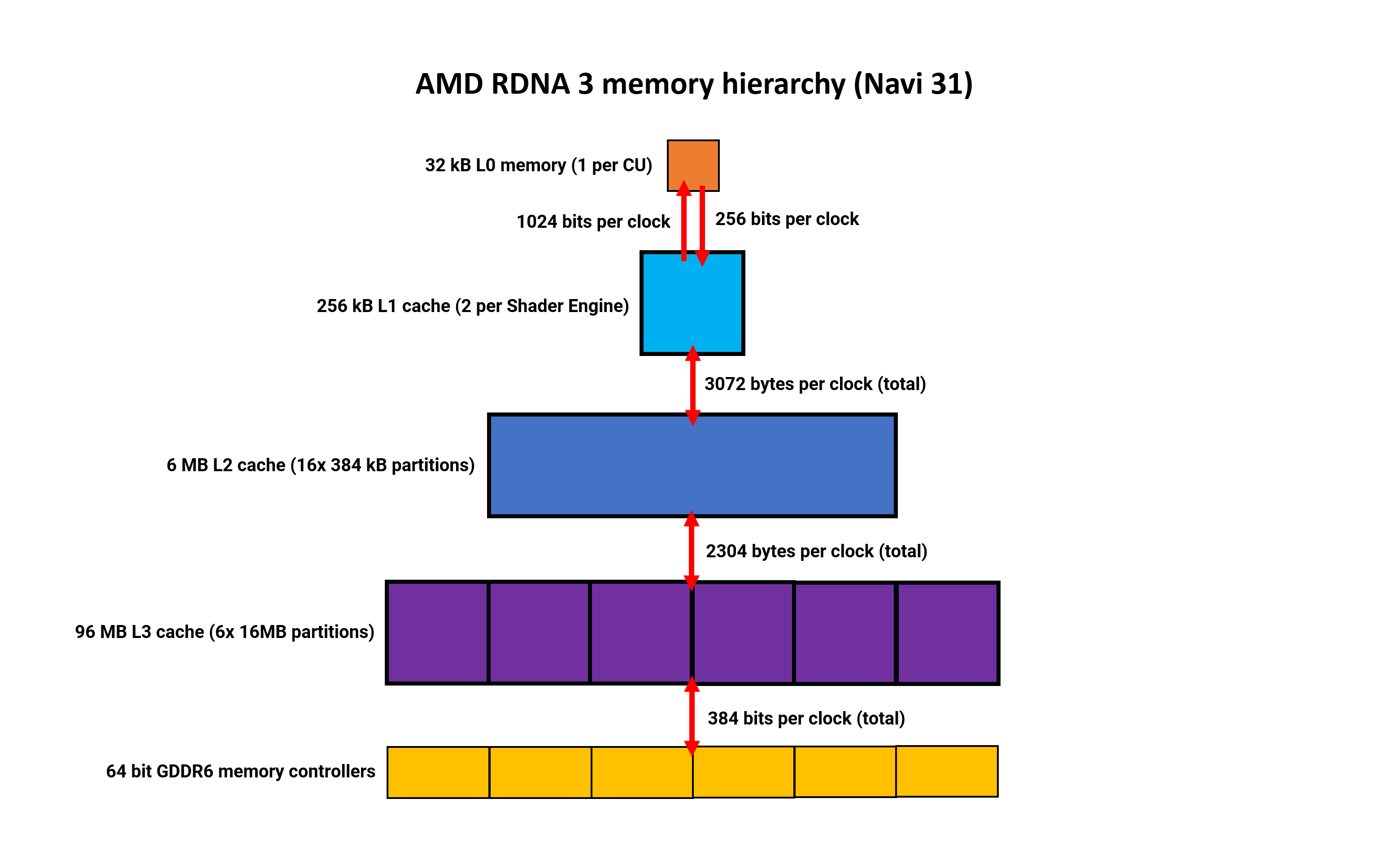
The register information at the moment are 50% bigger (which they needed to be, to deal with the rise in ALUs) and the primary three ranges of cache are all now bigger. L0 and L1 have doubled in measurement, and the L2 cache is as much as 2MB, to a complete of 6MB within the Navi 31 die.
The L3 cache has really shrunk to 96MB, however there is a good cause for this — it is not within the GPU die. We’ll discuss extra about that facet in a later part of this text.
With wider bus widths between the assorted cache ranges, the general inner bandwidth is so much greater too. Clock-for-clock, there’s 50% extra between L0 and L1, and the identical enhance between L1 and L2. But the largest enchancment is between L2 and the exterior L3 — it is now 2.25 instances wider, in complete.
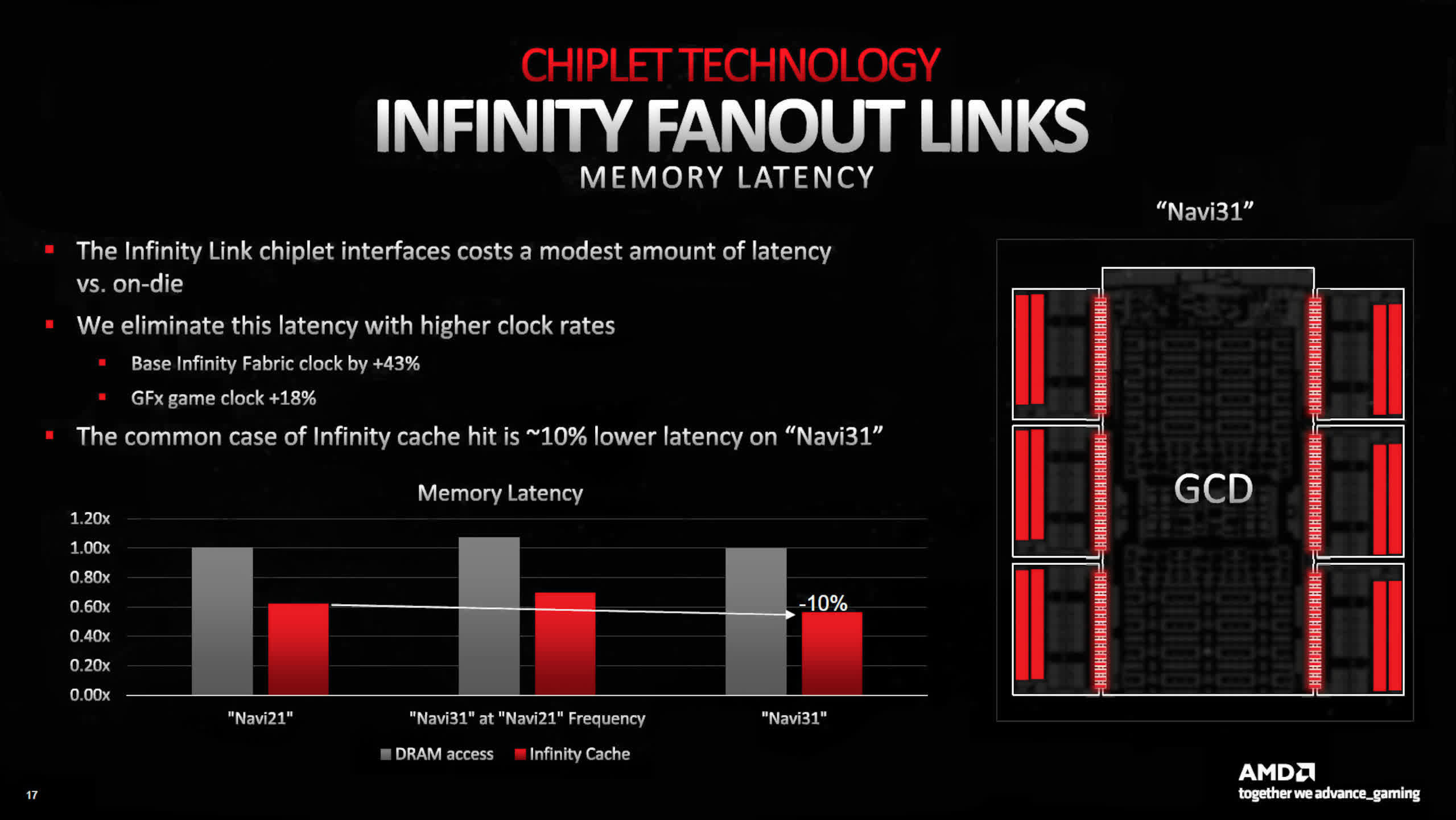
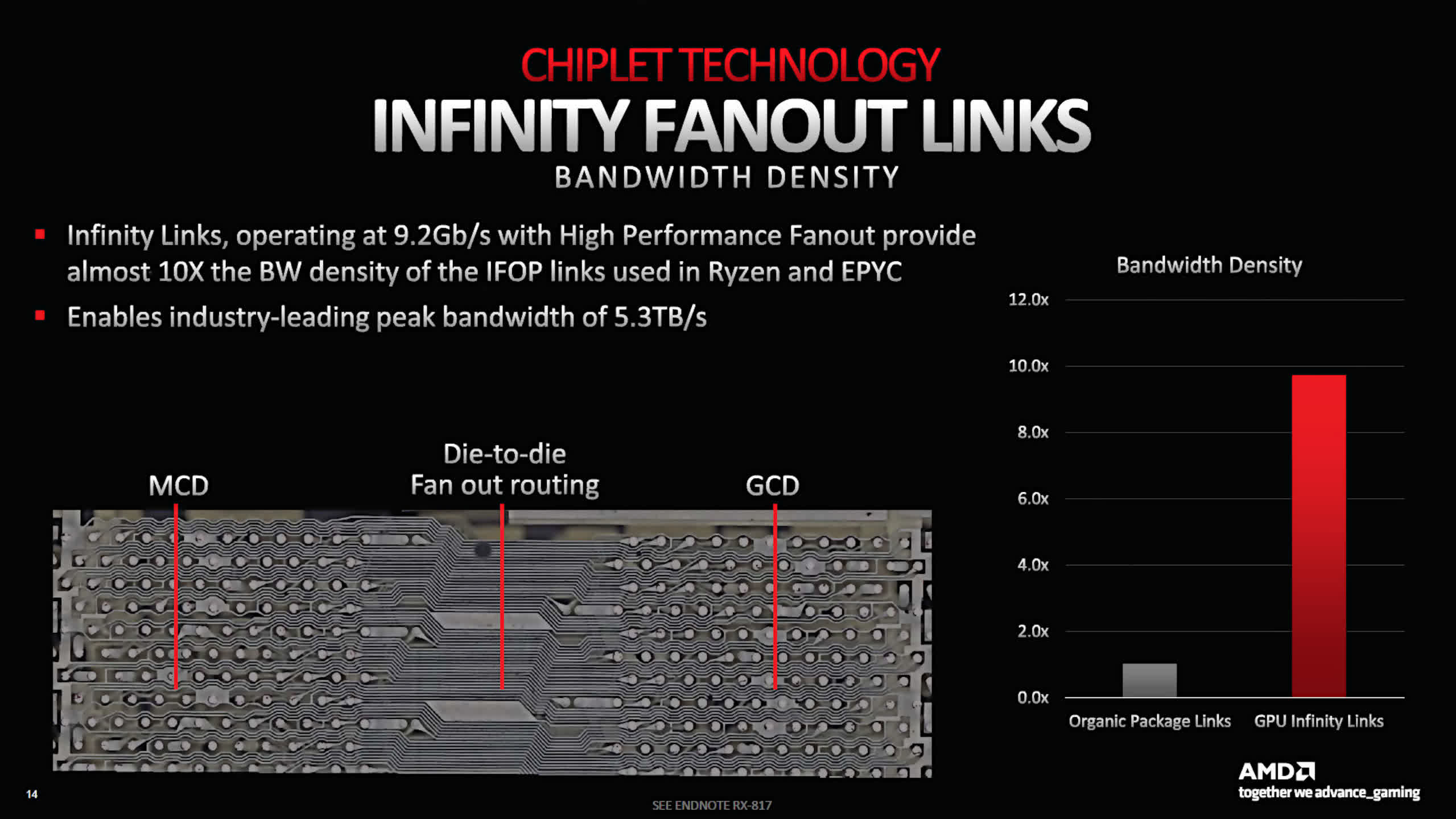
The Navi 21, as utilized in Radeon RX 6900 XT, had an L2-to-L3 complete peak bandwidth of two.3 TB/s; the Navi 31 within the Radeon RX 7900 XT will increase that to five.3 TB/s, resulting from the usage of AMD’s Infinity fanout hyperlinks.
Having the L3 cache separate from the principle die does enhance latency, however that is offset by way of greater clocks for the Infinity Fabric system — general, there is a 10% discount in L3 latency instances in comparison with RDNA 2.
RDNA 3 continues to be designed to make use of GDDR6, somewhat than the marginally quicker GDDR6X, however the top-end Navi 31 chip homes two extra reminiscence controllers to extend the worldwide reminiscence bus width to 384 bits.
AMD’s cache system is actually extra advanced than Intel’s and Nvidia’s, however micro-benchmarking of RDNA 2 by Chips and Cheese reveals that it is a very environment friendly system. The latencies are low throughout and it offers the background help required for the CUs to succeed in excessive utilization, so we will anticipate the identical of the system utilized in RDNA 3.
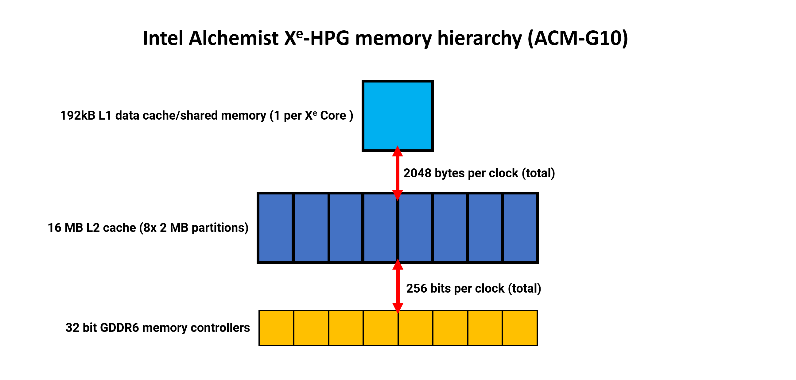
Intel’s reminiscence hierarchy is considerably less complicated, being primarily a two-tier system (ignoring smaller caches, similar to these for constants). There’s no L0 knowledge cache, only a first rate quantity 192kB of L1 knowledge & shared reminiscence.
Just as with Nvidia, this cache could be dynamically allotted, with as much as 128kB of it being accessible as shared reminiscence. Additionally, there is a separate 64kB texture cache (not proven in our diagram).
For a chip (the DG2-512 as used within the A770) that was designed for use in graphics playing cards for the mid-range market, the L2 cache may be very massive at 16MB in complete. The knowledge width is suitably huge, too, with a complete 2048 bytes per clock, between L1 and L2. This cache includes eight partitions, with every serving a single 32-bit GDDR6 reminiscence controller.
However, evaluation has proven that regardless of the wealth of cache and bandwidth on faucet, the Alchemist structure is not significantly good at absolutely utilizing all of it, requiring workloads with excessive thread counts to masks its comparatively poor latency.
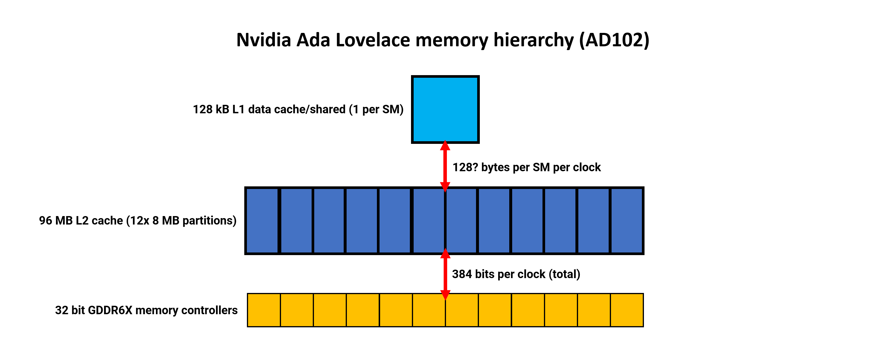
Nvidia has retained the identical reminiscence construction as utilized in Ampere, with every SM sporting 128kB of cache that acts as an L1 knowledge retailer, shared reminiscence, and texture cache. The quantity accessible for the completely different roles is dynamically allotted. Nothing has but been mentioned about any adjustments to the L1 bandwidth, however in Ampere it was 128 bytes per clock per SM. Nvidia has by no means been explicitly clear whether or not this determine is cumulative, combining learn and writes, or for one route solely.
If Ada is no less than the identical as Ampere, then the whole L1 bandwidth, for all SMs mixed, is a gigantic 18 kB per clock — far bigger than RDNA 2 and Alchemist.
But it should be pressured once more that the chips are usually not immediately comparable, as Intel’s was priced and marketed as a mid-range product, and AMD has made it clear that the Navi 31 was by no means designed to compete towards Nvidia’s AD102. Its competitor is the AD103 which is considerably smaller than the AD102.
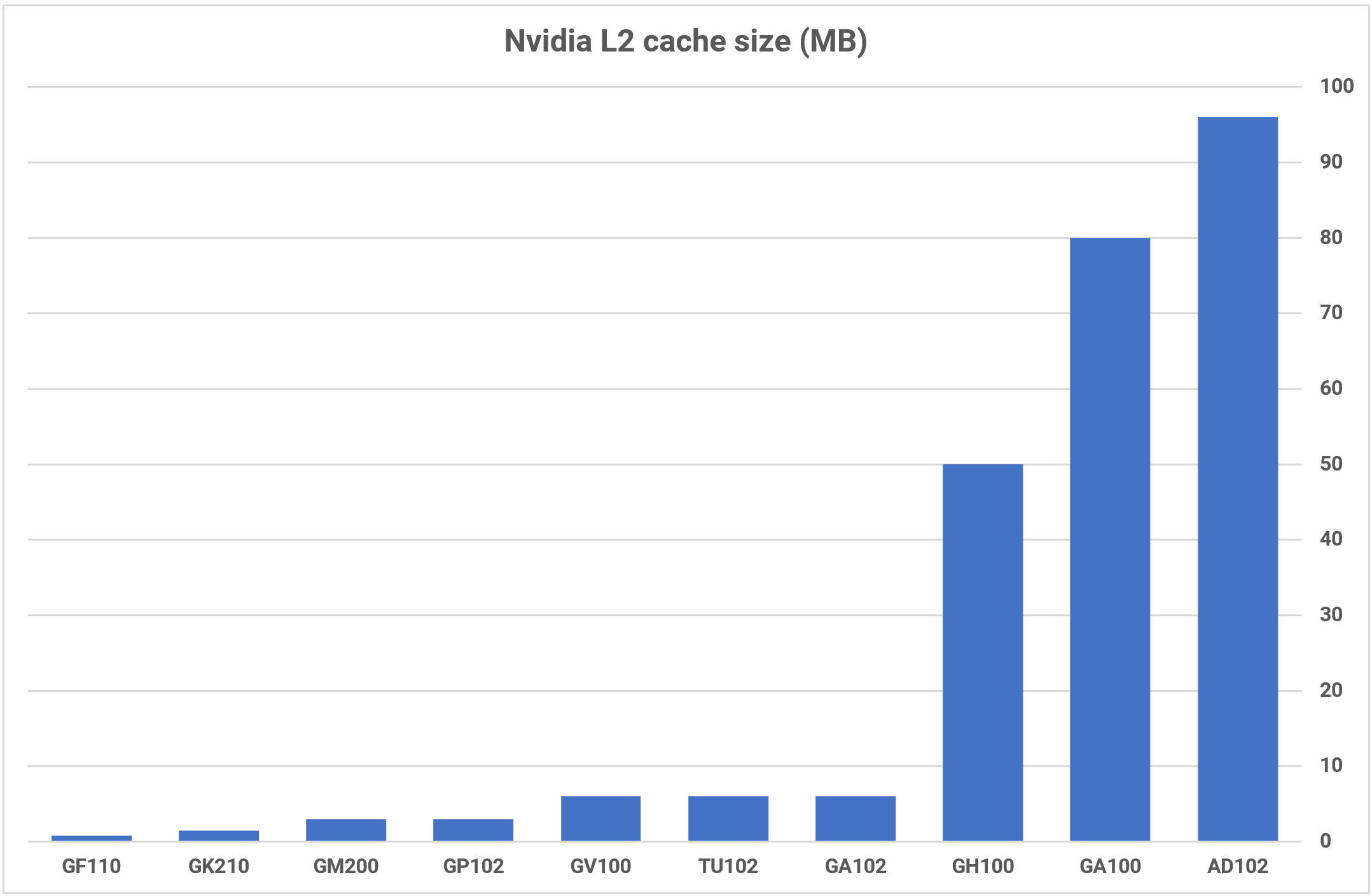
The greatest change to the reminiscence hierarchy is that the L2 cache has ballooned to 96MB, in a full AD102 die — 16 instances greater than its predecessor, the GA102. As with Intel’s system, the L2 is partitioned and paired with a 32-bit GDDR6X reminiscence controller, for a DRAM bus width of as much as 384 bits.
Larger cache sizes usually have longer latencies than smaller ones, however resulting from elevated clock speeds and a few enhancements with the buses, Ada Lovelace shows higher cache efficiency than Ampere.
If we examine all three techniques, Intel and Nvidia take the identical strategy for the L1 cache — it may be used as a read-only knowledge cache or as a compute shared reminiscence. In the case of the latter, the GPUs should be explicitly instructed, through software program, to make use of it on this format and the info is just retained for so long as the threads utilizing it are lively. This provides to the system’s complexity, but it surely produces a helpful enhance to compute efficiency.
In RDNA 3, the ‘L1’ knowledge cache and shared reminiscence are separated into two 32kB L0 vector caches and a 128kB native knowledge share. What AMD calls L1 cache can be a shared stepping stone, for read-only knowledge, between a gaggle of 4 DCUs and the L2 cache.
While not one of the cache bandwidths are as excessive as Nvidia’s, the multi-tiered strategy helps to counter this, particularly when the DCUs aren’t absolutely utilized.
Enormous, processor-wide cache techniques aren’t typically the most effective for GPUs, which is why we have not seen rather more than 4 or 6MB in earlier architectures, however the cause why AMD, Intel, and Nvidia all have substantial quantities within the ultimate tier is to counter the relative lack of development in DRAM speeds.
Adding a number of reminiscence controllers to a GPU can present loads of bandwidth, however at the price of elevated die sizes and manufacturing overheads, and options similar to HBM3 are much more costly to make use of.
We’ve but to see how effectively AMD’s system finally performs however their four-tiered strategy in RDNA 2 fared effectively towards Ampere, and it is considerably higher than Intel’s. However, with Ada packing in significantly extra L2, the competitors is not as easy.
Chip Packaging and Process Nodes: Different Ways to Build a Power Plant
There’s one factor that AMD, Intel, and Nvidia all have in widespread — all of them use TSMC to manufacture their GPUs.
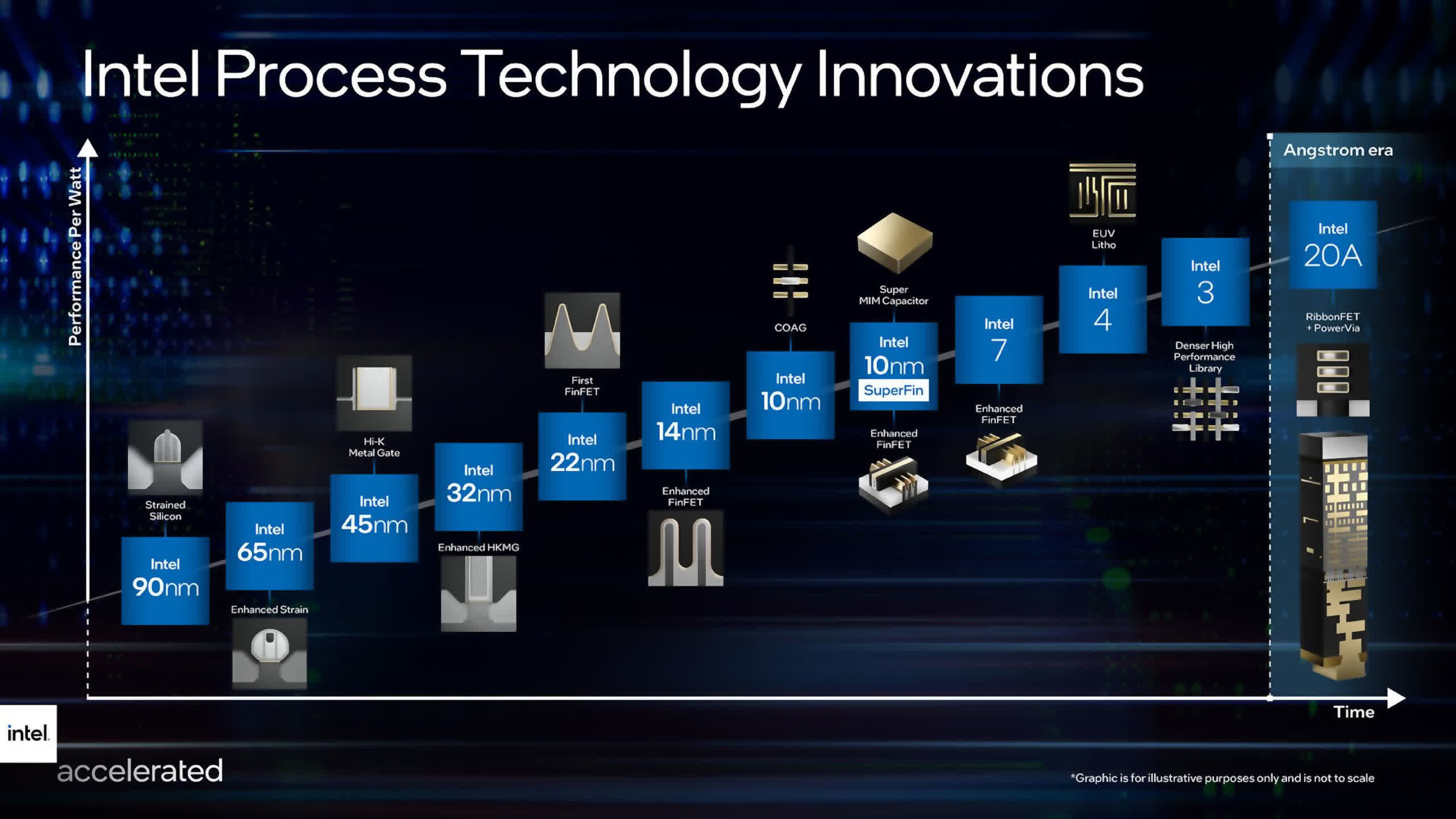
AMD makes use of two completely different nodes for the GCD and MCDs in Navi 31, with the previous made utilizing the N5 node and the latter on N6 (an enhanced model of N7). Intel additionally makes use of N6 for all its Alchemist chips. With Ampere, Nvidia used Samsung’s previous 8nm course of, however with Ada they switched again to TSMC and its N4 course of, which is a variant of N5.
N4 has the best transistor density and the most effective performance-to-power ratio of all of the nodes, however when AMD launched RDNA 3, they highlighted that solely logic circuitry has seen any notable enhance in density.
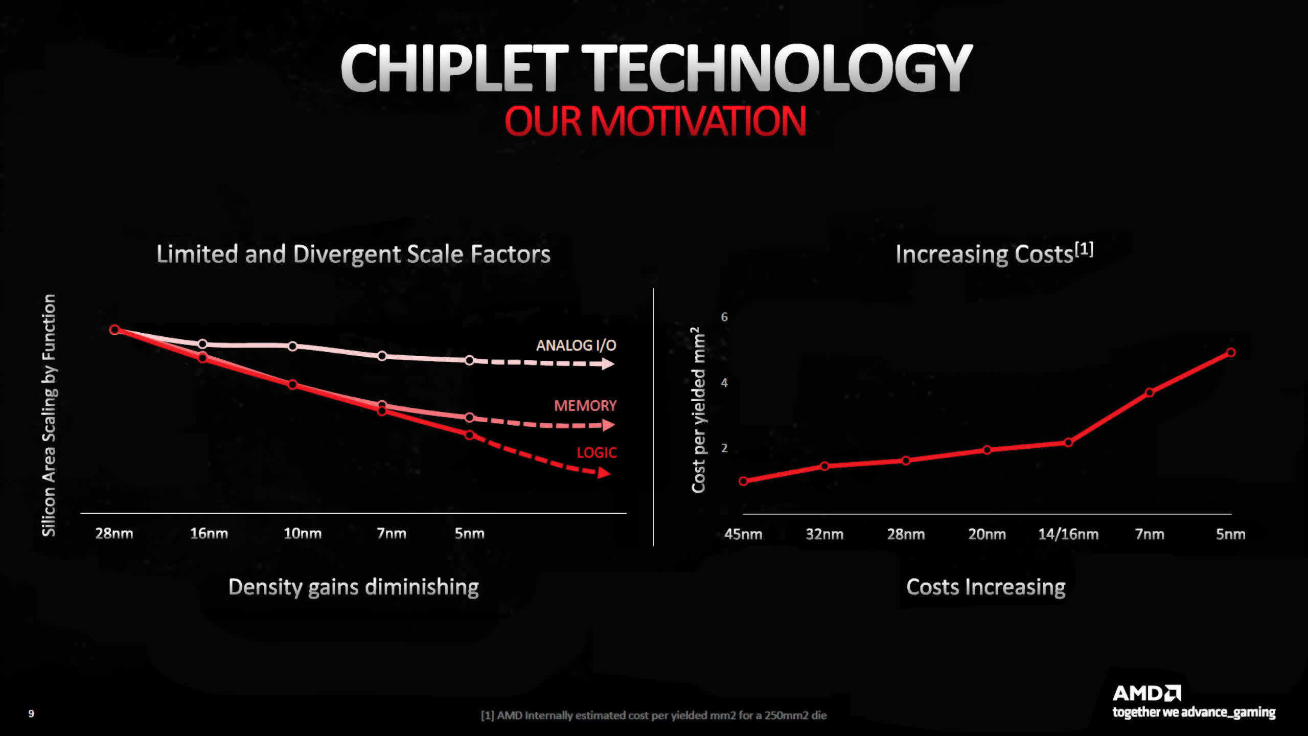
SRAM (used for cache) and analog techniques (used for reminiscence, system, and different signaling circuits) have shrunk comparatively little. Coupled with the rise in value per wafer for the newer course of nodes, AMD made the choice to make use of the marginally older and cheaper N6 to manufacture the MCDs, as these chiplets are largely SRAM and I/O.
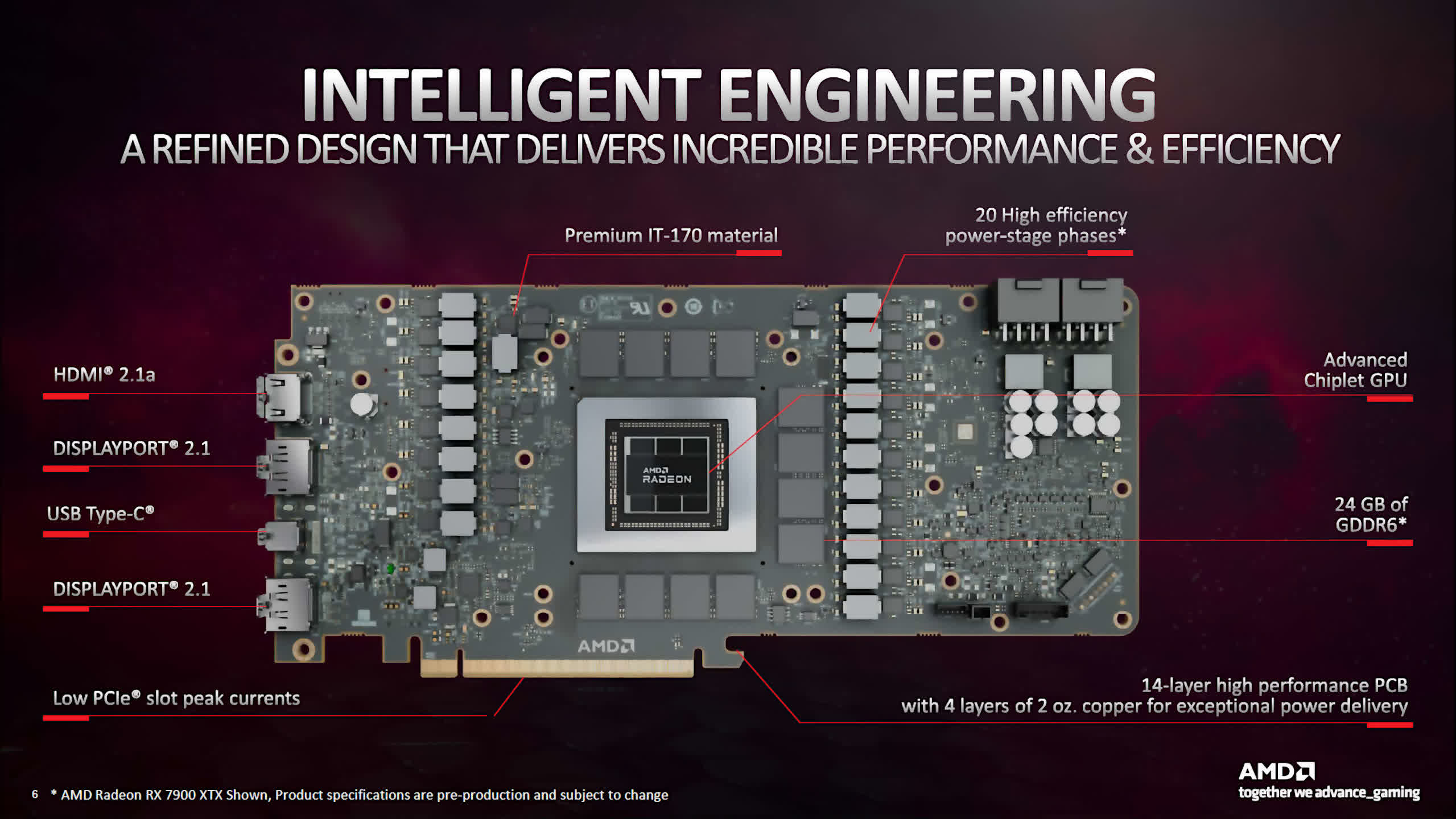
In phrases of die measurement, the GCD is 42% smaller than the Navi 21, coming in at 300 mm2. Each MCD is simply 37mm2, so the mixed die space of the Navi 31 is roughly the identical as its predecessor. AMD has solely said a mixed transistor rely, for all of the chiplets, however at 58 billion, this new GPU is their ‘largest’ client graphics processor ever.
To join every MCD to the GCD, AMD is utilizing what they name High Performance Fanouts — densely packed traces, that take up a really small quantity of area. The Infinity Links — AMD’s proprietary interconnect and signaling system — run at as much as 9.2Gb/s and with every MCD having a hyperlink width of 384 bits, the MCD-to-GCD bandwidth involves 883GB/s (bidirectional).
That’s equal to the worldwide reminiscence bandwidth of a high-end graphics card, for only a single MCD. With all six within the Navi 31, the mixed L2-to-MCD bandwidth comes to five.3TB/s.
The use of advanced fanouts means the price of die packaging, in comparison with a standard monolithic chip, goes to be greater however the course of is scalable — completely different SKUs can use the identical GCD however various numbers of MCDs. The smaller sizes of the person chiplet dies ought to enhance wafer yields, however there is not any indication as as to if AMD has included any redundancy into the design of the MCDs.
If there is no, it means any chiplet that has flaws within the SRAM, which stop that a part of the reminiscence array from getting used, then they should be binned for a lower-end mannequin SKU or not used in any respect.
AMD has solely introduced two RDNA 3 graphics playing cards up to now (Radeon RX 7900 XT and XTX), however in each fashions, the MCDs area 16MB of cache every. If the subsequent spherical of Radeon playing cards sports activities a 256 bit reminiscence bus and, say, 64MB of L3 cache, then they might want to use the ‘excellent’ 16MB dies, too.
However, since they’re so small in space, a single 300mm wafer might doubtlessly yield over 1500 MCDs. Even if 50% of these must be scrapped, that is nonetheless adequate dies to furnish 125 Navi 31 packages.
It will take a while earlier than we will inform simply how cost-effective AMD’s design really is, however the firm is absolutely dedicated to utilizing this strategy now and sooner or later, although just for the bigger GPUs. Budget RNDA 3 fashions, with far smaller quantities of cache, will proceed to make use of a monolithic fabrication technique because it’s more cost effective to make them that approach.
Intel’s ACM-G10 processor is 406mm2, with a complete transistor rely of 21.7 billion, sitting someplace between AMD’s Navi 21 and Nvidia’s GA104, by way of element rely and die space.
This really makes it fairly a big processor, which is why Intel’s selection of market sector for the GPU appears considerably odd. The Arc A770 graphics card, which makes use of a full ACM-G10 die, was pitched towards the likes of Nvidia’s GeForce RTX 3060 — a graphics card that makes use of a chip half the scale and transistor rely of Intel’s.
So why is it so massive? There are two possible causes: the 16MB of L2 cache and the very massive variety of matrix items in every XEC. The resolution to have the previous is logical, because it eases strain on the worldwide reminiscence bandwidth, however the latter might simply be thought of extreme for the sector it is bought in. The RTX 3060 has 112 Tensor cores, whereas the A770 has 512 XMX items.
Another odd selection by Intel is the usage of TSMC N6 for manufacturing the Alchemist dies, somewhat than their very own services. An official assertion given on the matter cited components similar to value, fab capability, and chip working frequency.
This means that Intel’s equal manufacturing services (utilizing the renamed Intel 7 node) would not have been in a position to meet the anticipated demand, with their Alder and Raptor Lake CPUs taking over a lot of the capability.
They would have in contrast the relative drop in CPU output, and the way that may have impacted income, towards what they’d have gained with Alchemist. In brief, it was higher to pay TSMC to make its new GPUs.
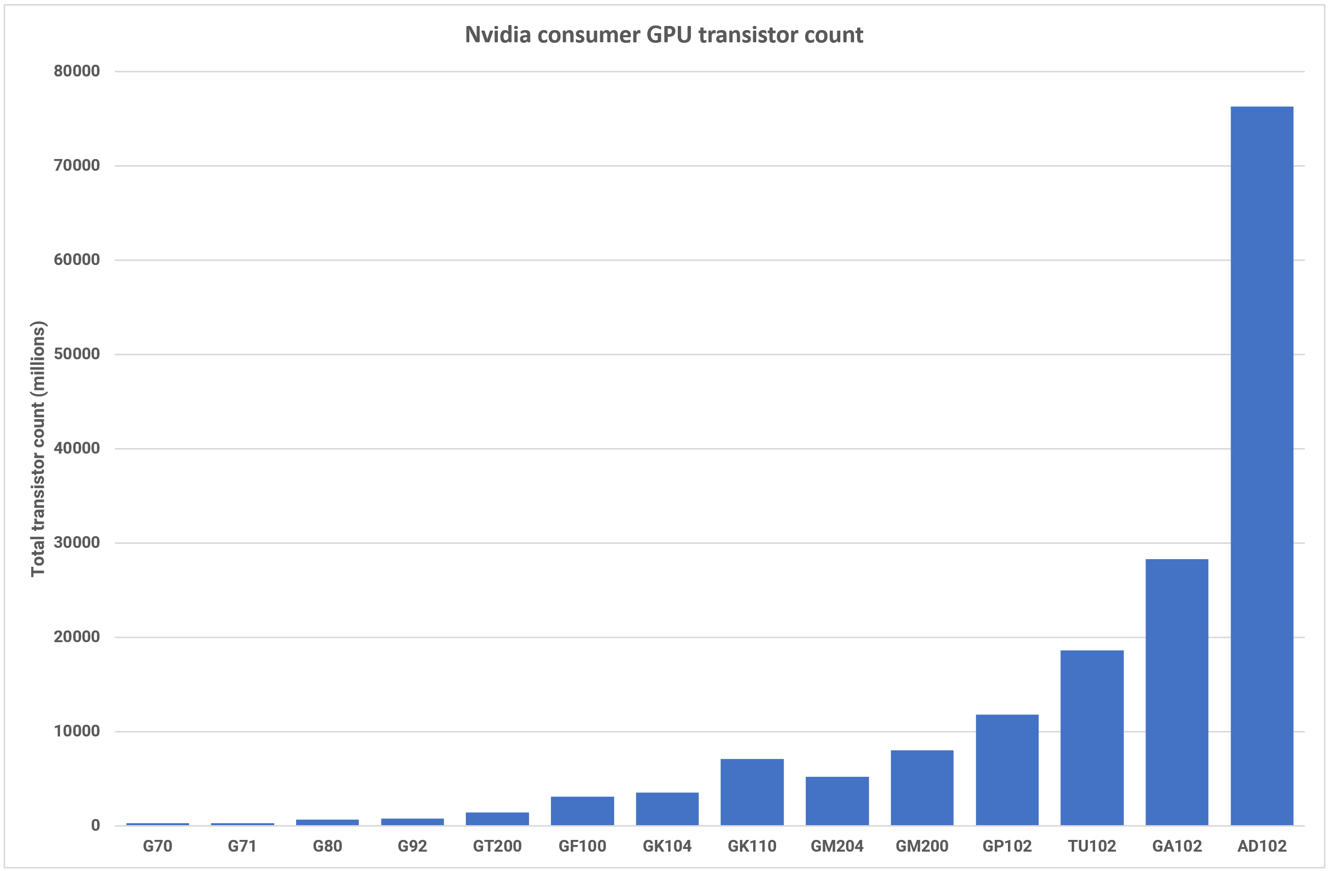
Where AMD used its multichip experience and developed new applied sciences for the manufacture of enormous RDNA 3 GPU, Nvidia caught with a monolithic design for the Ada lineup. The GPU firm has appreciable expertise in creating extraordinarily massive processors, although at 608mm2 the AD102 is not the bodily largest chip it has launched (that honor goes to the GA100 at 826mm2).
However, with 76.3 billion transistors, Nvidia has pushed the element rely approach forward of any consumer-grade GPU seen up to now.
The GA102, used within the GeForce RTX 3080 and upwards, appears light-weight as compared, with simply 26.8 billion. This 187% enhance went in the direction of the 71% development in SM rely and the 1500% uplift in L2 cache quantity.
Such a big and complicated chip as this can at all times battle to realize excellent wafer yields, which is why earlier top-end Nvidia GPUs have spawned a mess of SKUs. Typically, with a brand new structure launch, their skilled line of graphics playing cards (e.g. the A-series, Tesla, and so on) are introduced first.
When Ampere was introduced, the GA102 appeared in two consumer-grade playing cards at launch and went on to finally discovering a house in 14 completely different merchandise. So far, Nvidia has up to now chosen to make use of AD102 in simply two: the GeForce RTX 4090 and the RTX 6000. The latter hasn’t been accessible for buy since showing in September, although.
The RTX 4090 makes use of dies which are in the direction of the higher finish of the binning course of, with 16 SMs and 24MB of L2 cache disabled, whereas the RTX 6000 has simply two SMs disabled. Which leaves one to ask: the place are the remainder of the dies?
But with no different merchandise utilizing the AD102, we’re left to imagine that Nvidia is stockpiling them, though for what different merchandise is not clear.
The GeForce RTX 4080 makes use of the AD103, which at 379mm2 and 45.9 billion transistors, is nothing like its larger brother — the a lot smaller die (80 SMs, 64MB L2 cache) ought to end in much better yields, however once more there’s solely the one product utilizing it.
They additionally introduced one other RTX 4080, one utilizing the smaller-still AD104, however back-tracked on that launch as a result of weight of criticism they obtained. It’s anticipated that this GPU will now be used to launch the RTX 4070 lineup.
Nvidia clearly has loads of GPUs constructed on the Ada structure but in addition appears very reluctant to ship them. One cause for this might be that they are ready for Ampere-powered graphics playing cards to clear the cabinets; one other is the truth that it dominates the overall consumer and workstation markets, and presumably feels that it would not want to supply anything proper now.
But given the substantial enchancment in uncooked compute functionality that each the AD102 and 103 supply, it is considerably puzzling that there are so few Ada skilled playing cards — the sector is at all times hungry for extra processing energy.
Superstar DJs: Display and Media Engines
When it involves the media & show engines of GPUs, they usually obtain a back-of-the-stage advertising strategy, in comparison with elements similar to DirectX 12 options or transistor rely. But with the sport streaming trade producing billions of {dollars} in income, we’re beginning to see extra effort being made to develop and promote new show options.
For RDNA 3, AMD up to date various parts, probably the most notable being help for DisplayPort 2.1 (in addition to HDMI 2.1a). Given that VESA, the group that oversees the DisplayPort specification, solely introduced the two.1 model just a few months in the past, it was an uncommon transfer for a GPU vendor to undertake the system so shortly.
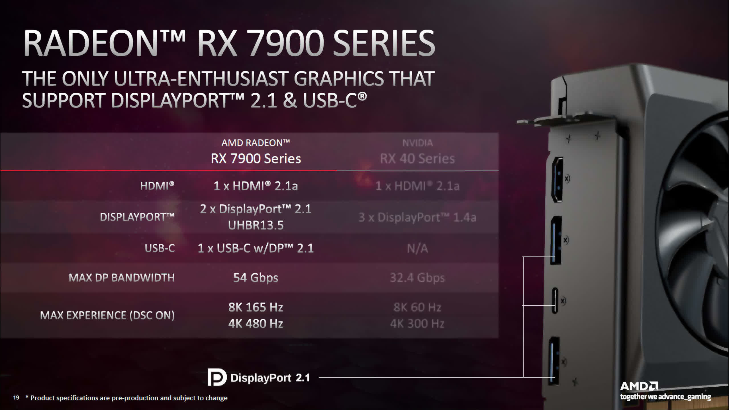
The quickest DP transmission mode the brand new show engine helps is UHBR13.5, giving a most 4-lane transmission fee of 54 Gbps. This is nice sufficient for a decision of 4K, at a refresh fee of 144Hz, with none compression, on commonplace timings.
Using DSC (Display Stream Compression), the DP2.1 connections allow as much as 4K@480Hz or 8K@165Hz — a notable enchancment over DP1.4a, as utilized in RDNA 2.
Intel’s Alchemist structure includes a show engine with DP 2.0 (UHBR10, 40 Gbps) and HDMI 2.1 outputs, though not all Arc-series graphics playing cards utilizing the chip could make the most of the utmost capabilities.
While the ACM-G10 is not focused at high-resolution gaming, the usage of the most recent show connection specs signifies that e-sports displays (e.g. 1080p, 360Hz) can be utilized with none compression. The chip could not have the ability to render such excessive body charges in these sorts of video games, however no less than the show engine can.

AMD and Intel’s help for quick transmission modes in DP and HDMI is the type of factor you’d anticipate from brand-new architectures, so it is considerably incongruous that Nvidia selected not to take action with Ada Lovelace.
The AD102, for all its transistors (virtually the identical as Navi 31 and ACM-G10 added collectively), solely has a show engine with DP1.4a and HDMI 2.1 outputs. With DSC, the previous is nice sufficient for, say, 4K@144Hz, however when the competitors helps that with out compression, it is clearly a missed alternative.
Media engines in GPUs are liable for the encoding and decoding of video streams, and all three distributors have fulsome function units of their newest architectures.
In RDNA 3, AMD added full, simultaneous encode/decode for the AV1 format (it was decode solely within the earlier RDNA 2). There’s not a substantial amount of details about the brand new media engines, apart from it could possibly course of two H.264/H.265 streams on the identical time, and the utmost fee for AV1 is 8K@60Hz. AMD additionally briefly talked about ‘AI Enhanced’ video decode however supplied no additional particulars.
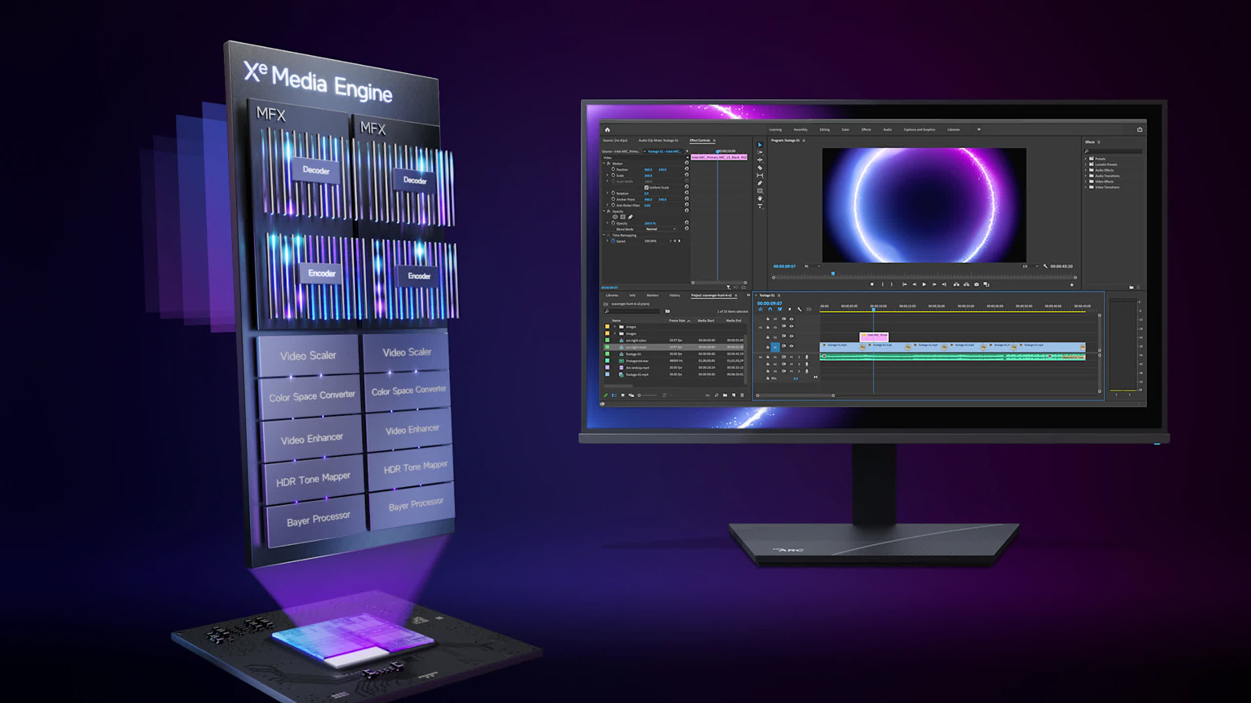
Intel’s ACM-G10 has the same vary of capabilities, encode/decoding accessible for AV1, H.264, and H.265, however simply as with RDNA 3, particulars are very scant. Some early testing of the primary Alchemist chips in Arc desktop graphics playing cards means that the media engines are as least pretty much as good as these provided by AMD and Nvidia of their earlier architectures.
Ada Lovelace follows swimsuit with AV1 encoding and decoding, and Nvidia is claiming that the brand new system is 40% extra environment friendly in encoding than H.264 — ostensibly, 40% higher video high quality is offered when utilizing the newer format.
Top-end GeForce RTX 40 sequence graphics playing cards will include GPUs sporting two NVENC encoders, supplying you with the choice of encoding 8K HDR at 60Hz or improved parallelization of video exporting, with every encoder engaged on half a body on the identical time.
With extra details about the techniques, a greater comparability might be made, however with media engines nonetheless being seen because the poor relations to the rendering and compute engines, we’ll have to attend till each vendor has playing cards with their newest architectures on cabinets, earlier than we will look at issues additional.
What’s Next for the GPU?
It’s been a very long time since we have had three distributors within the desktop GPU market and it is clear that every one has its personal strategy to designing graphics processors, although Intel and Nvidia take the same mindset.
For them, Ada and Alchemist are considerably of a jack-of-all-trades, for use for every kind of gaming, scientific, media, and knowledge workloads. The heavy emphasis on matrix and tensor calculations within the ACM-G10 and a reluctance to utterly redesign their GPU format reveals that Intel is leaning extra in the direction of science and knowledge, somewhat than gaming, however that is comprehensible, given the potential development in these sectors.
With the final three architectures, Nvidia has centered on enhancing upon what was already good, and lowering numerous bottlenecks inside the general design, similar to inner bandwidth and latencies. But whereas Ada is a pure refinement of Ampere, a theme that Nvidia has adopted for various years now, the AD102 stands out as being an evolutionary oddity if you have a look at the sheer scale of the transistor rely.
The distinction in comparison with the GA102 is nothing wanting outstanding, however this colossal leap raises various questions. The first of which is, would the AD103 have been a more sensible choice for Nvidia to go together with, for his or her highest-end client product, as an alternative of the AD102?
As used within the RTX 4080, AD103’s efficiency is a good enchancment over the RTX 3090, and like its larger brother, the 64MB of L2 cache helps to offset the comparatively slim 256-bit world reminiscence bus width.
And at 379mm2, it is smaller than the GA104 used within the GeForce RTX 3070, so could be much more worthwhile to manufacture than the AD102. It additionally homes the identical variety of SMs because the GA102 and that chip finally discovered a house in 15 completely different merchandise.
Another query price asking is, the place does Nvidia go from right here by way of structure and fabrication? Can they obtain the same stage of scaling, whereas nonetheless sticking to a monolithic die?
AMD’s selections with RDNA 3 spotlight a possible route for the competitors to comply with. By shifting the elements of the die that scale the worst (in new course of nodes) into separate chiplets, AMD has been in a position to efficiently proceed the massive fab & design leap made between RDNA and RDNA 2.
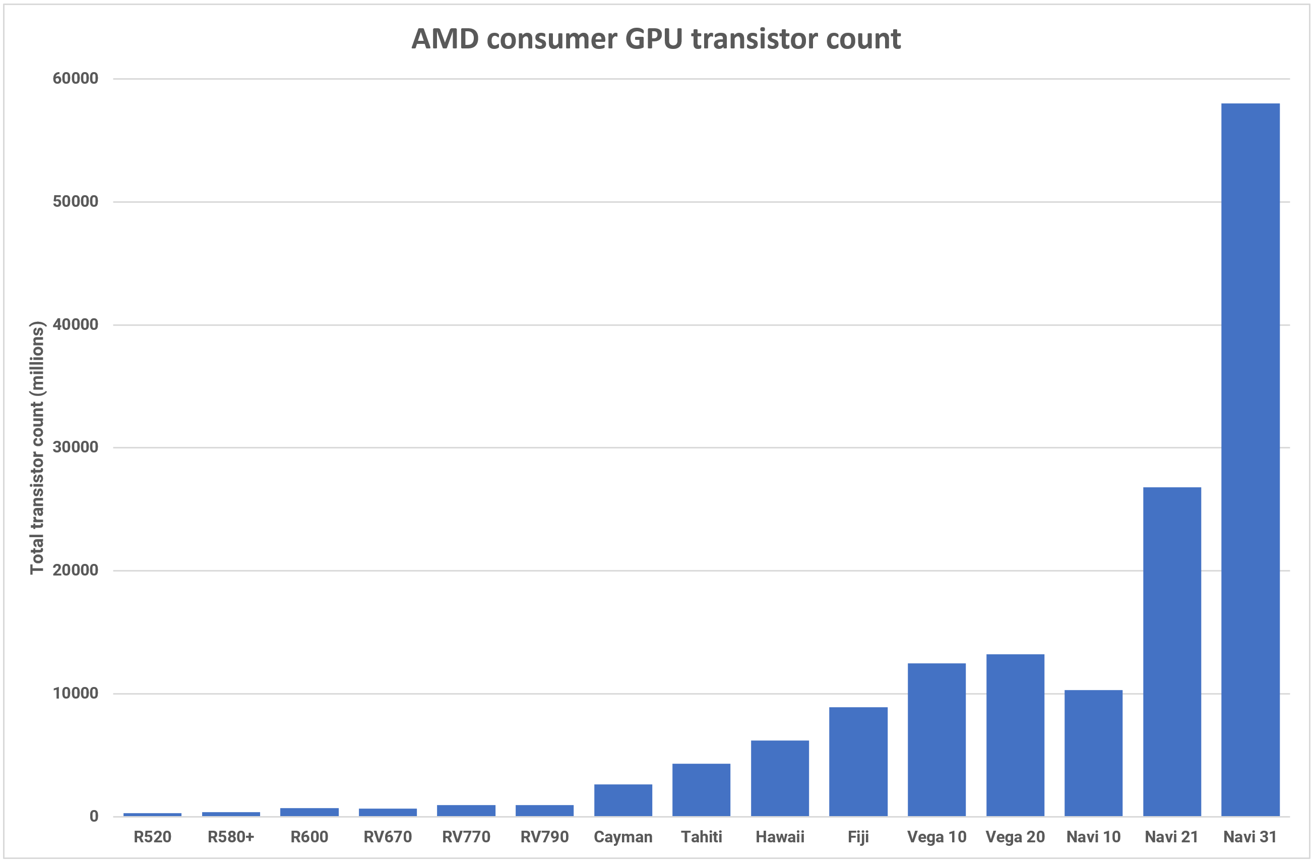
While it isn’t as massive because the AD102, the Navi 31 continues to be 58 billion transistors price of silicon — greater than double that in Navi 21, and over 5 instances that within the authentic RDNA GPU, the Navi 10 (though that wasn’t aimed to be a halo product).
But AMD and Nvidia’s achievements weren’t accomplished in isolation. Such massive will increase in GPU transistor counts are solely attainable due to the fierce competitors between TSMC and Samsung for being the premier producer of semiconductor gadgets.
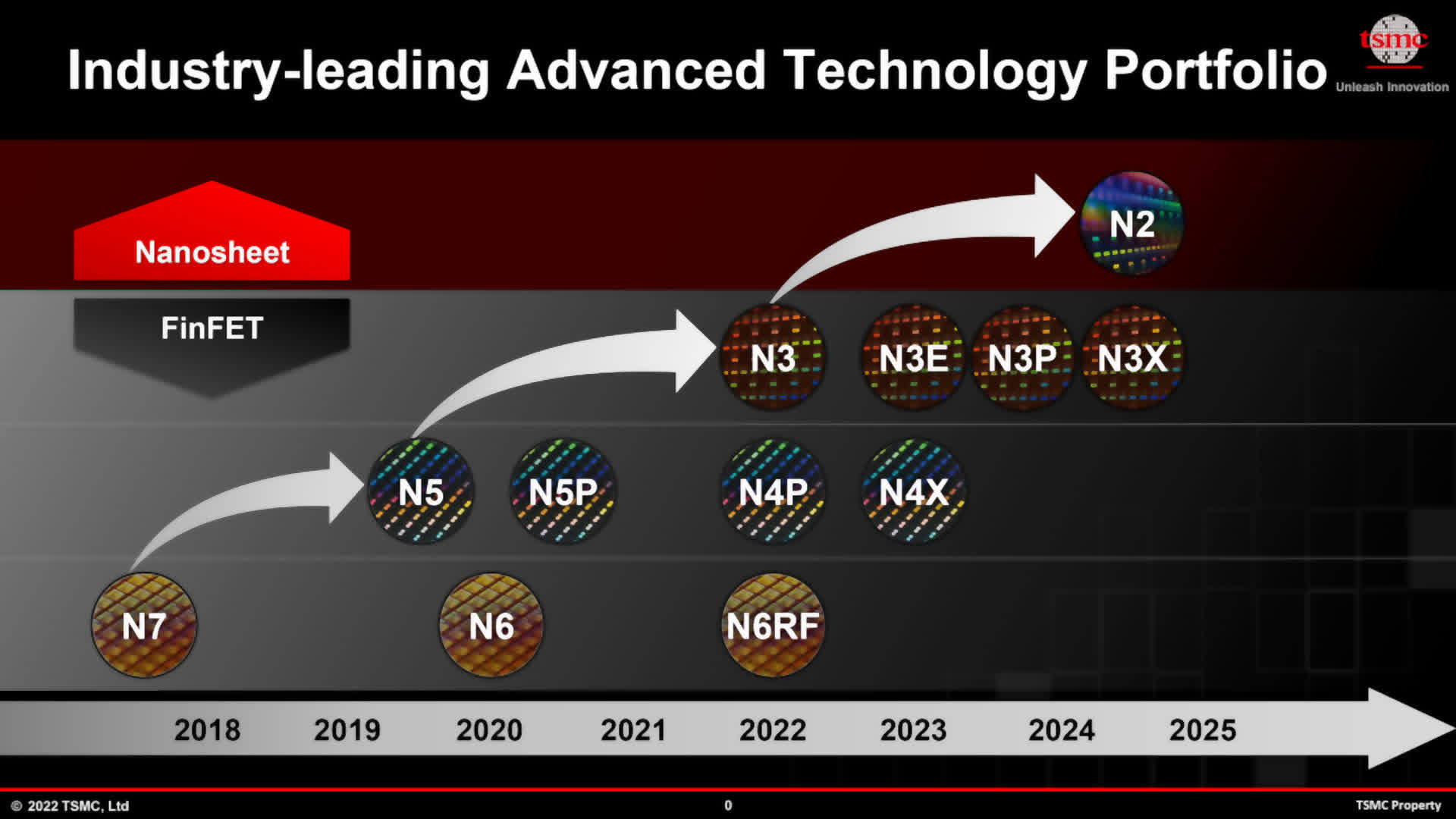
Both are working in the direction of enhancing the transistor density of logic circuits, whereas persevering with to cut back energy consumption, with Samsung commencing quantity manufacturing of its 3nm course of earlier this yr. TSMC has been doing likewise and has a transparent roadmap for present node refinements and their subsequent main course of.
Whether Nvidia copies a leaf from AMD’s design e-book and goes forward with a chiplet format in Ada’s successor is unclear, however the subsequent 14 to 16 months will most likely be decisive. If RDNA 3 proves to be a monetary success, be it by way of income or complete items shipped, then there is a distinct risk that Nvidia follows swimsuit.
However, the primary chip to make use of the Ampere structure was the GA100 — an information middle GPU, 829mm2 in measurement and with 54.2 billion transistors. It was fabricated by TSMC, utilizing their N7 node (the identical as RDNA and a lot of the RDNA 2 lineup). The use of N4, to make the AD102, allowed Nvidia to design a GPU with virtually double the transistor density of its predecessor.
GPUs proceed to be one of the crucial outstanding engineering feats seen in a desktop PC
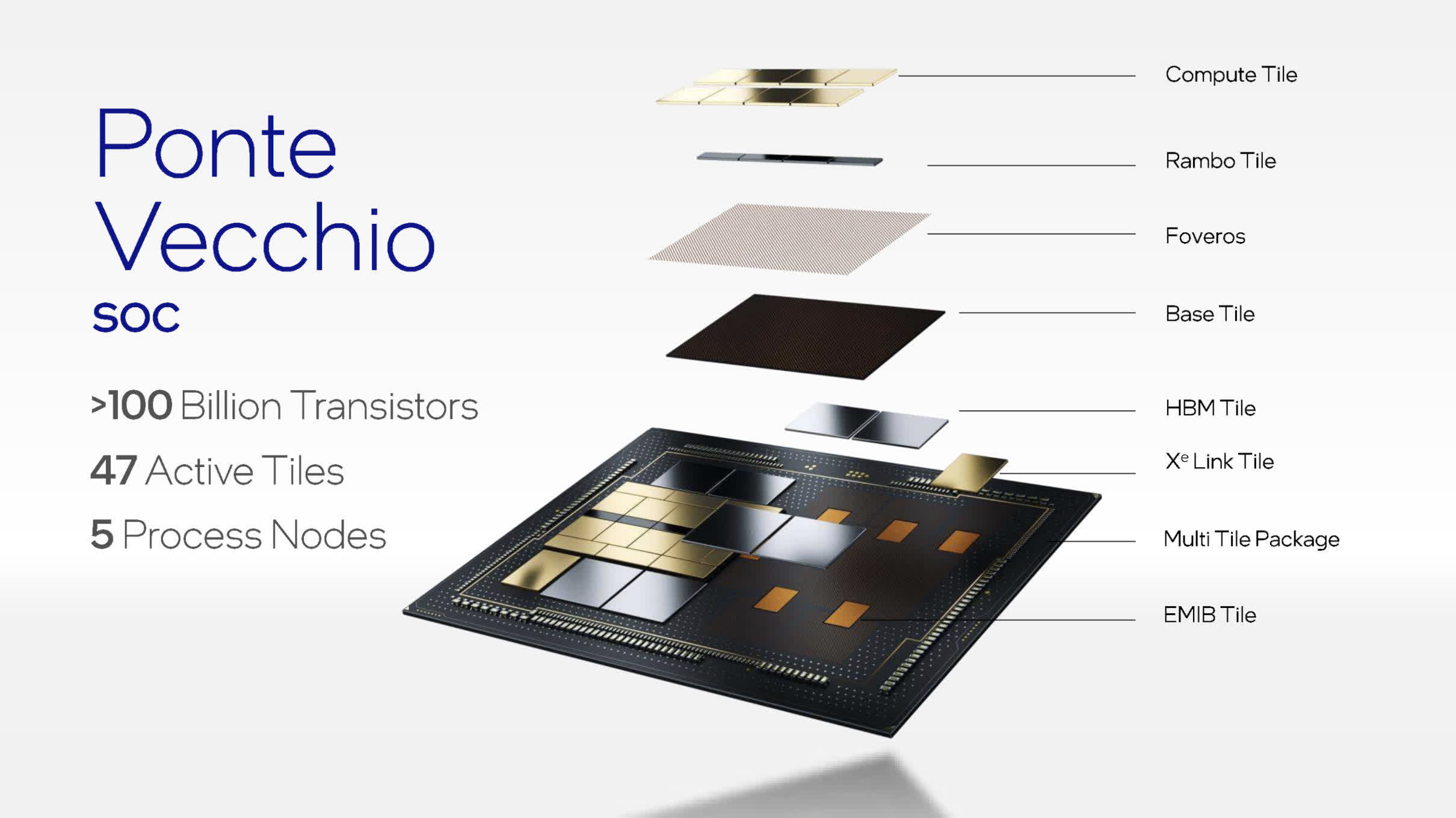
So would this be achievable utilizing N2 for the subsequent structure? Possibly, however the huge development in cache (which scales very poorly) means that even when TSMC achieves some outstanding figures with their future nodes, it is going to be more and more tougher to maintain GPU sizes underneath management. Intel already is utilizing chiplets, however solely with its huge Ponte Vecchio knowledge middle GPU. Composed of 47 numerous tiles, some fabrication by TSMC and others by Intel themselves, its parameters are suitably extreme.
For instance, with greater than 100 billion transistors for the total, dual-GPU configuration, it makes AMD’s Navi 31 look svelte. It is, in fact, not for any sort of desktop PC neither is it strictly talking ‘simply’ a GPU — this can be a knowledge middle processor, with a agency emphasis on matrix and tensor workloads.
With its Xe-HPG structure focused for no less than two extra revisions (Battlemage and Celestial) earlier than transferring on to ‘Xe Next’, we could effectively see the usage of tiling in an Intel client graphics card.
For now, although, we’ll have Ada and Alchemist, utilizing conventional monolithic dies, for no less than a yr or two, whereas AMD makes use of a mix of chiplet techniques for the upper-mid and top-end playing cards, and single dies for his or her finances SKUs.
By the tip of the last decade, although, we may even see virtually every kind of graphics processors, constructed from a choice of completely different tiles/chiplets, all made utilizing numerous course of nodes. GPUs proceed to be one of the crucial outstanding engineering feats seen in a desktop PC — transistor counts present no signal of tailing off in development and the computational skills of a mean graphics card at this time might solely be dreamed about 10 years in the past.
Bring on the subsequent three-way structure battle!