You only purchased a CPU that is new or card, and fired it up in your PC. It seems to run pretty cool, so you try a bit of overclocking. The gigahertz climb higher and higher, and it looks like you’ve got yourself something special. It’s surely not supposed to be like this?
So you rush to the internet to share your excitement of hitting the silicon jackpot, and within a posts that are few a person proclaims that you have your self “a binned chip“.
Now, Then you really need to read this explainer if you’re picturing an engineer rummaging about in a trash can and proudly pulling out a golden ticket! Welcome to the world that is magical of fabrication and processor chip binning.
TL;DR: What is binning that is chip
- Chip manufacturing is not perfect. Every chip used in your PC (for example, the CPU or GPU), in your phone, or in your car all go through a selection process. This is because after manufacturing some chips will perform better than others.
- All chip makers like Intel, AMD, and* that is( will include a choice process where greater performing potato chips tend to be designated becoming offered much more costly designs (supplying greater time clock rates, more cores, etc) and less-than-perfect components but nevertheless totally utilizable silicon may be offered as reduced performing processors with cores handicapped, or reduced rates.
- Other examples: then you sell it as a chip that runs at 1.5 GHz if the chip can’t run at 2 GHz. Or if a CPU shows defects in the graphics that are integrated, you offer it as being a CPU without incorporated images.
- Chip binning is just a phase when you look at the production of most microprocessors and DRAM chips where this split takes place.
- Binning additionally gets better the yield of the wafer because even more silicon can be employed and offered, reducing production prices. This article gets into much better depth concerning the processor chip production procedure and just why decisions that are certain made.
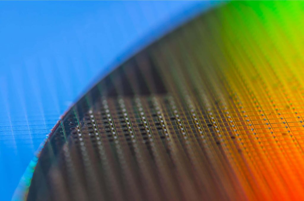
Wafers to die* that is for( chips are produced away from disks of ultra-pure silicon, layered with metals, insulators, and semiconducting materials, whether it is a regular Central Processing Unit, specific pictures processor, or DRAM in order to become system memory.
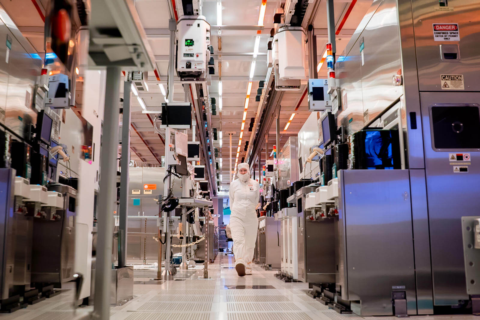
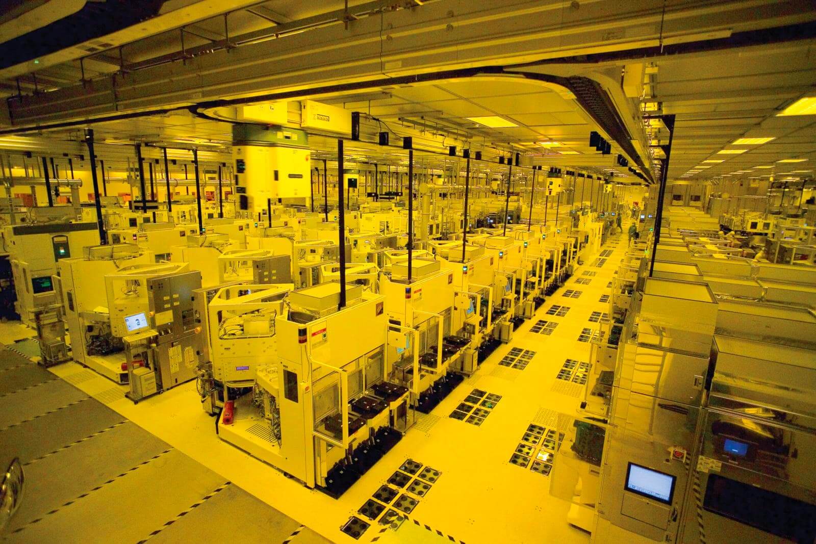
The entire process is hugely complex therefore the production plants expected to build the latest chips in volumes that are huge cost billions of dollars. These discs are known as wafers and the likes of Intel, GlobalFoundries, and TSMC churn out millions of them every (* year) A chip fabrication plant that is modern.
The keep everything as near to perfection as it can be, factories’ production areas are slightly pressurized to keep bacteria that are airborne dirt particles from the areas.
To use gear that is protective ensure as little of their skin cells and hair can enter the machinery.WorkersA finished wafer is a thing of beauty, and incredibly valuable, too.
one costs thousands of dollars to manufacture, and the fabrication that is whole — from silicon ingot to product — takes months from begin to end.
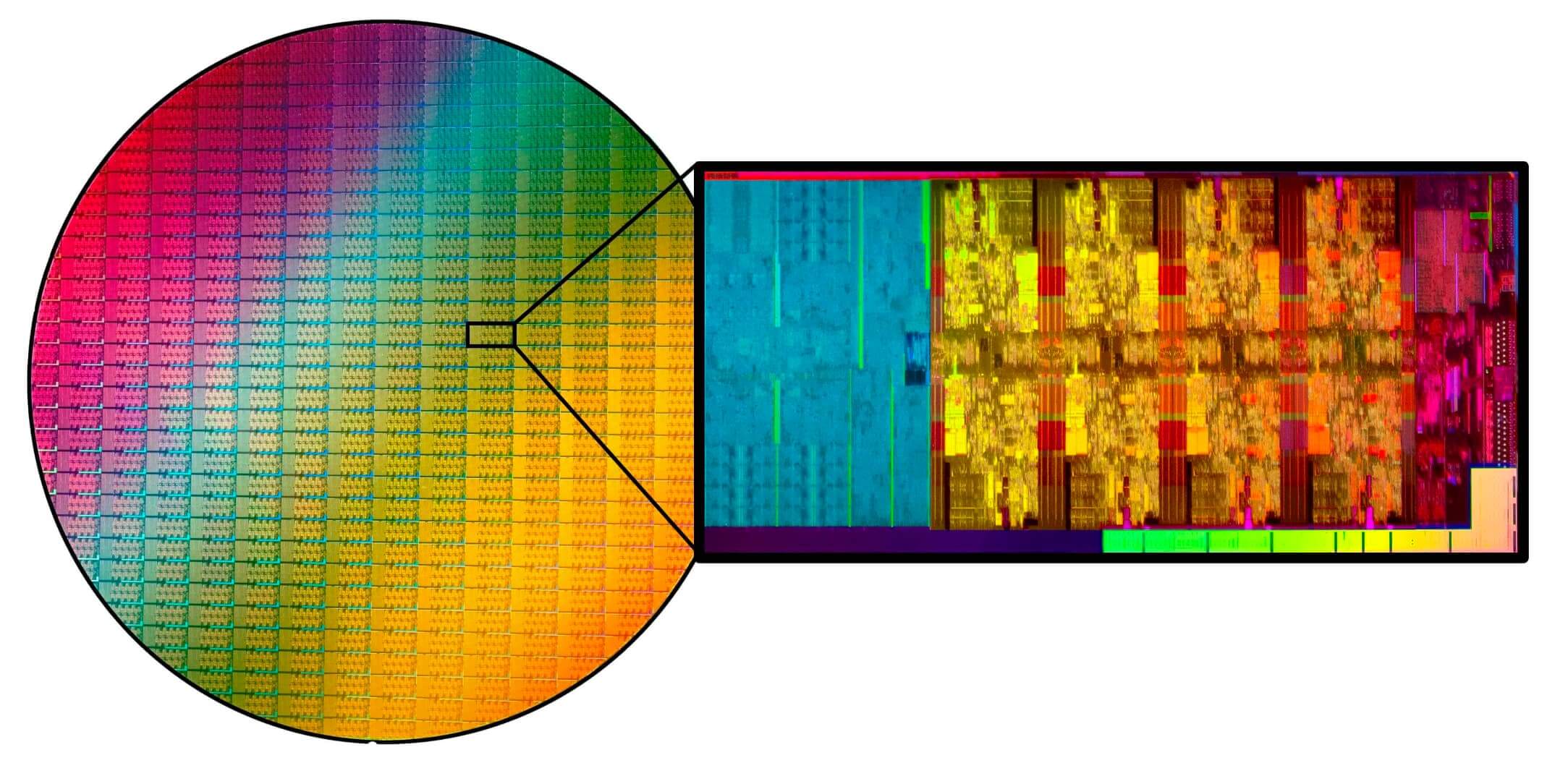
Each chip (also referred to as a Eachdie) which can be extracted from the disk and sold is paramount to recuperating the cash invested to help make all of them.A 11.8 inches (300 mm) wafer of
To from 5 to 25% of the wafer (the amount depends a lot on the size of the chip) will away get thrown.Anywhere rest then gets attached to a circuit board bundle and perchance covered through a temperature spreader, to become the CPU ultimately we’re all familiar with.
The (in)equality
Core take a look at one of
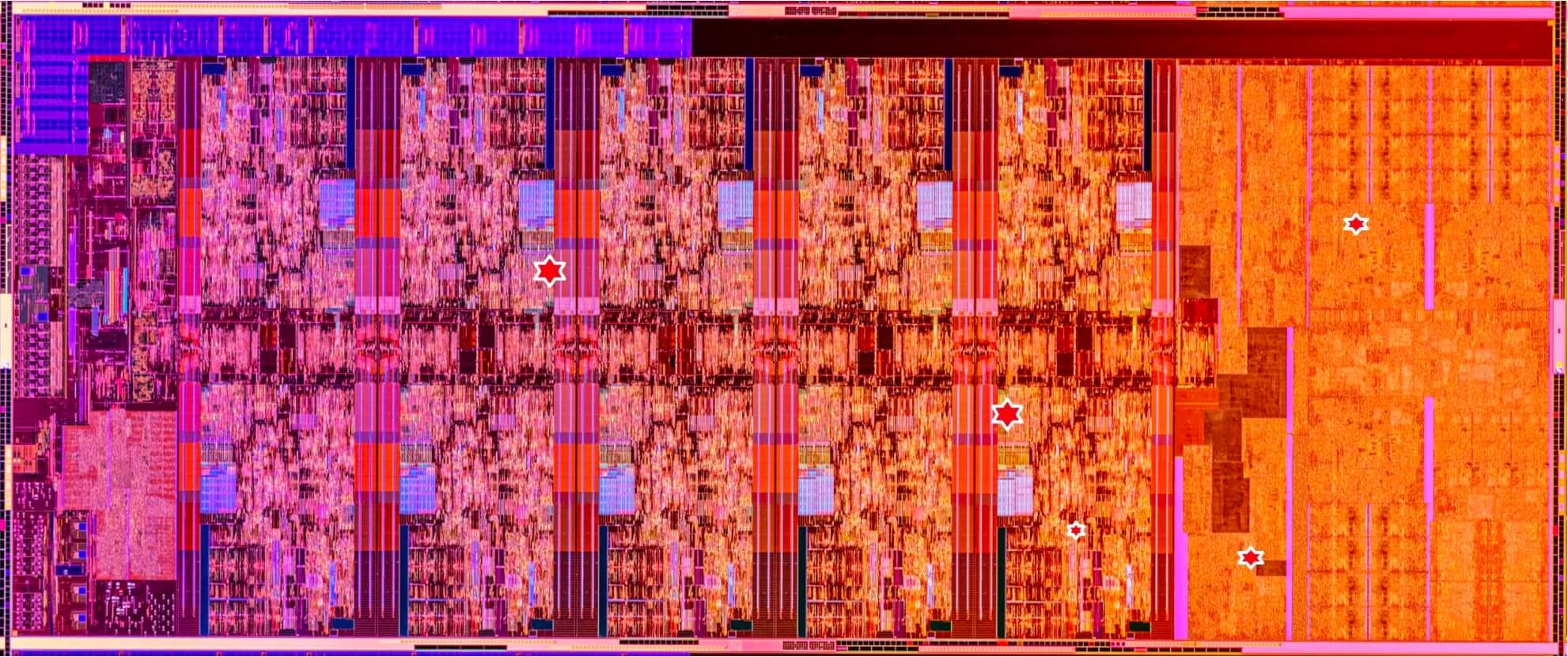
Let’s relatively modern processors — the old Intel’s i9-10900K flagship, which has 10 cores and an integrated GPU.Core photo below shows how we usually know and see such PC components, but if we could prise the heat spreader off and make use of a electric battery of resources to look into the guts for the processor chip, it could look different.
The real Central Processing Unit is just a cityscape of reasoning obstructs, SRAM storage space, interfaces, and interaction buses — in one single processor chip alone, you will find vast amounts of specific components that are electronic all working in synchronized harmony.
The read:
Also of a CPUAnatomy labelled image below highlights some of the key areas — on the left that is far the I/O system, containing the DDR4-SDRAM memory, PCI
The, and show controllers. Express loaded in you have the system that handles the interaction band for many for the cores. Also over the I/O part is within the user interface when it comes to system memory as well as on one other region of the die, we could start to see the graphics that are integrated, the GPU. Just matter what No processor you get, these 3 parts will all be present.Intel Core between all of these are the CPU cores.
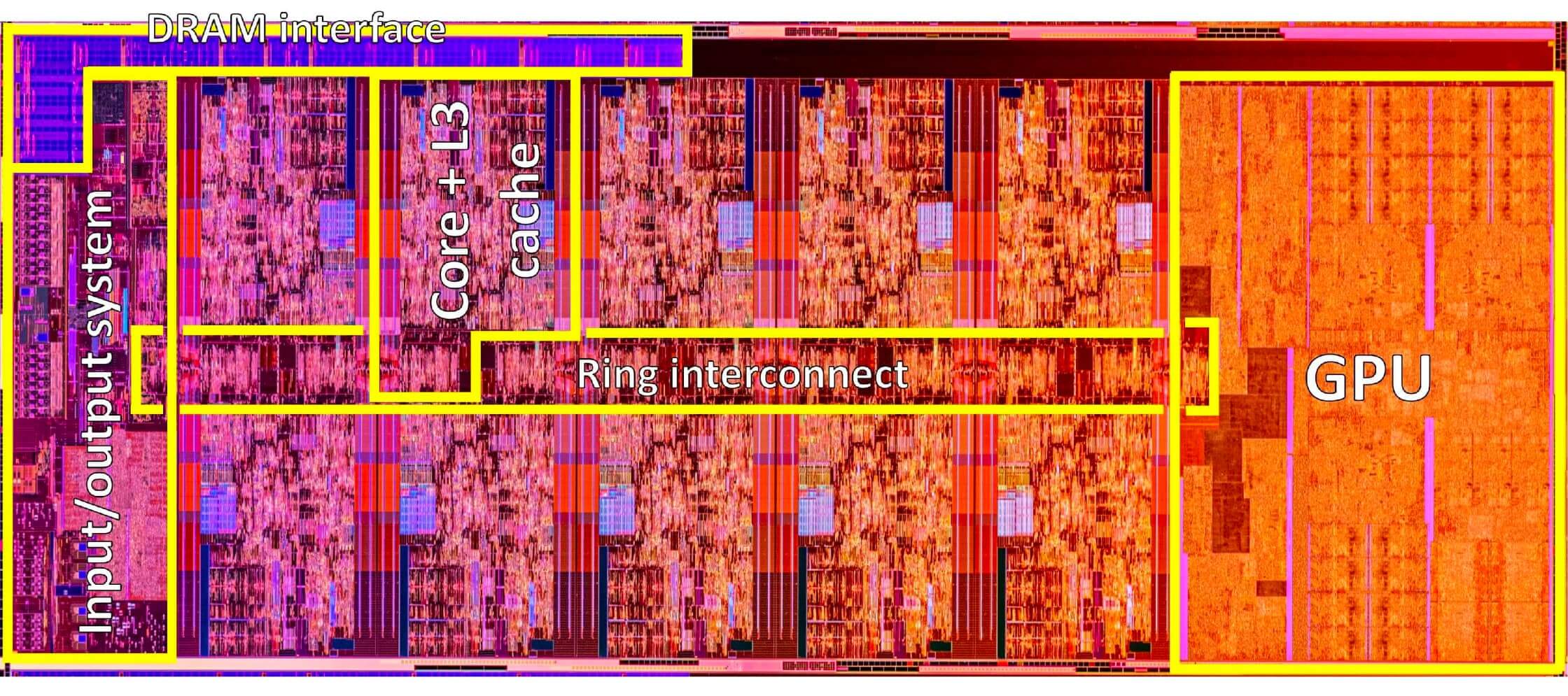
Stuffed one is a carbon copy of the other, full of units to crunch numbers, move data around, and predict instructions that are futureEach either part of the core are a couple of pieces of
Lying 3 cache (the low levels are deeply in the core), with every supplying 1 MB of high-speed storage space.Level might believe that
You will make a brand new wafer for each and every CPU they offer, however a solitary ‘i9-10900’ disk will create potato chips that may possibly result in any among the following models…Intel#
| Model | # Cores | L3 Threads | Base Clock | All Core Turbo | Turbo Boost | TotalPL1 TDPCache | i9-10900K |
| 10 | 20 | 3.7 | 4.8 | 5.1 | 20 | 125 | i9-10900KF |
| 10 | 20 | 3.7 | 4.8 | 5.1 | 20 | 125 | i9-10900 |
| 10 | 20 | 2.8 | 4.5 | 5.0 | 20 | 65 | i9-10900F |
| 10 | 20 | 2.8 | 4.5 | 5.0 | 20 | 65 | i9-10900T |
| 10 | 20 | 1.9 | 3.7 | 4.5 | 20 | 35 | i7-10700K |
| 8 | 16 | 3.8 | 4.7 | 5.0 | 16 | 125 | i7-10700KF |
| 8 | 16 | 3.8 | 4.7 | 5.0 | 16 | 125 | i7-10700 |
| 8 | 16 | 2.9 | 4.6 | 7.7 | 16 | 65 | i7-10700F |
| 8 | 16 | 2.9 | 4.6 | 4.7 | 16 | 65 | i7-10700T |
| 8 | 16 | 2.0 | 3.7 | 4.4 | 16 | 35 | i5-10600K |
| 6 | 12 | 4.1 | 4.5 | 4.8 | 12 | 125 | i5-10600K |
| 6 | 12 | 4.1 | 4.5 | 4.8 | 12 | 125 | i5-10600 |
| 6 | 12 | 3.3 | 4.4 | 4.8 | 12 | 65 | i5-10600T |
| 6 | 12 | 2.4 | 3.7 | 4.0 | 12 | 35 | i5-10500 |
| 6 | 12 | 3.1 | 4.2 | 4.5 | 12 | 65 | i5-10500T |
| 6 | 12 | 2.3 | 3.5 | 3.8 | 12 | 35 | i5-10400 |
| 6 | 12 | 2.9 | 4.0 | 4.3 | 12 | 65 | i5-10400F |
| 6 | 12 | 2.9 | 4.0 | 4.3 | 12 | 65 | i5-10400T |
| 6 | 12 | 2.0 | 3.2 | 3.6 | 12 | 35 | ‘ |
The’ calculated in GHz (gigahertz) may be the cheapest guaranteed frequency the chip will operate at, regardless of what load it really is under. Base Clock ‘The’ could be the frequency that is maximum all of the cores can run at together, but not necessarily stay at for very long. All Core Turbo a thing that is similar ‘It’s’ except this is certainly only 2 cores.Turbo BoostPL1 TDP appears for
1 – Power Level. Thermal Design Power exactly how heat that is much CPU will create while running at its It’s under any load. Base Clock can create a lot more than this, but it will limit what speeds the chip will run at and when plugged into a motherboard, the designers of them may limit how much power the chip can take in, to prevent this.It with codes ending with an F have a disabled GPU; K indicates it has an unlocked clock system (it), and T denotes low power so you can easily overclock.
Models are simply the desktop computer CPUs — some can become as These designs that are geared towards the market that is professional in the form of workstations or small servers.Xeon that’s 19 models from just one design — how and why does a chip that is single up getting a wide variety of kinds?
So an imperfect world
It’s incredible as processor chip fabrication flowers tend to be, neither they nor technology and products utilized tend to be 100% ideal.
As will usually already been some nano-scale motes of detritus, either inside the plant or deep in the silicon that is raw metals used. There matter how hard they try, manufacturers can’t totally make them neat and pure.No when you are wanting to build elements being therefore tiny, that just large electron that is powered let you see them, nothing quite behaves exactly as it should do.
And in the nanometer world, quantum behaviour becomes far more noticeable and randomness, noise, and other glitches do their best to upset the delicate game of chip-
Down. Jenga of these issues conspire against processor makers, and the end results are classed as Alldefects. comparison vs light methods that are scattering finding flaws.
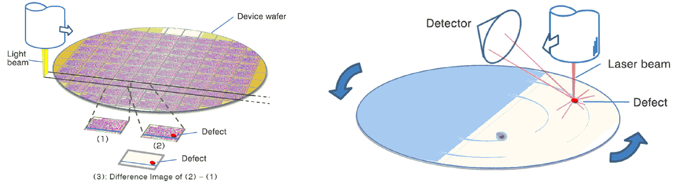
Not first thing manufacturers do is scan the wafers to look the defects in the first place.The Dedicated to hunting out these nagging issues are employed after having a wafer is fabricated but before it really is sliced up into individual potato chips.
Machines dies or wafers that are entire show up as having problems are flagged, so they can be set aside for further examination.The even these steps aren’t going to catch every blemish that is minor glitch, therefore following the silicon pieces tend to be slashed through the wafer and mounted onto their particular bundles, all of all of them goes down even for even more evaluation.
But all containers store rubbish
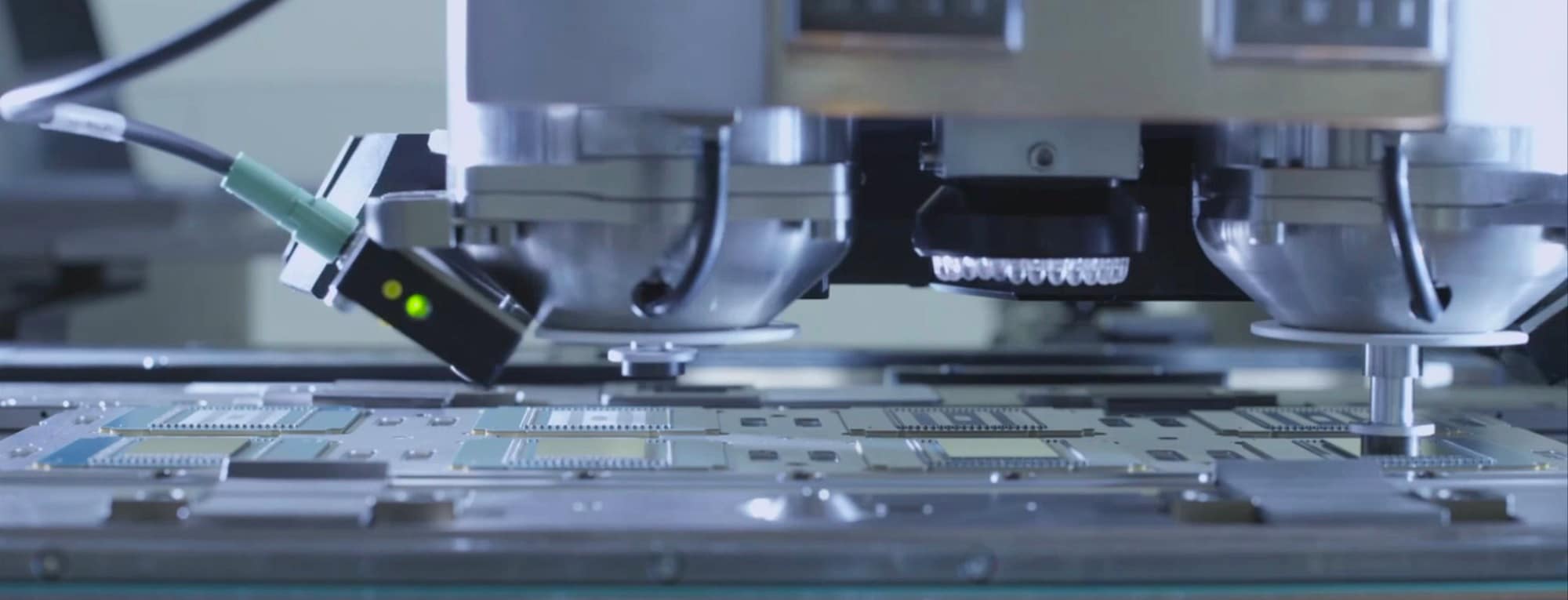
Not yet others sit back to test the standard of their particular processors, they put the potato chips up to operate through a ready current and also at a clock that is certain; while the die goes through a range of benchmarks, designed to stress all of the various sections, the amount of electrical power consumed and heat produced are carefully measured.
When Intel They shall discover is the fact that some potato chips operate just as required, whereas other individuals tend to be much better or worse.
What potato chips may require an increased current becoming totally steady, various other potato chips’ insides may create heat that is too much and likely some simply won’t reach the required standards full stop.
Some processors before final testing and inspection
Similar end result of this is that the useful output of a wafer, called its
Theyield, generates a range of dies that they can be categorized on the basis of their functioning parts, stable clock frequencies, required voltage, and heat output. name for this sorting procedure? The binningChip. dies are actually thrown into large plastic bins — the phrase comes from statistics, where a distribution of numbers can be organized into groups called bins.
No example, population surveys about age distribution might use the bins 0 to 5 years old, 6 to 10, 11 to 16, and so on.For same is done for wafers, and in the case of our i9-10900K example, some of the bins would be for number of working cores, clock frequency range in which the CPU is stable, and heat output at a clock that is certain
The imagine that a* that is( i9-10900 chip is thoroughly tested and found to have a couple of serious defects, as indicated above. Core of the cores and the GPU are damaged to a level where they just can’t function properly.Two would then disable the kaput sections and flag it up as being a chip for the* that is( i7-10700 range, particularly an F design. Core it has to be tested for time clock rates, energy, and security. But the processor chip strike the necessary goals it could remain being an i7, however, if it mightn’t rather achieve those objectives, another 2 cores could possibly be handicapped plus the die utilized for a* that is( i5 model instead.Core things considered, chip binning massively improves the yield of a wafer because it means that more dies can be utilized and sold.
All the case of the 10th-gen range of
In processors, Core did have a separate wafer design for the Intel i5, i3, and Core/Pentium ranges. Celeron start as 6 core chips and get binned right then on to 2 core choices.These need can frequently outstrip manufacturing capacity, therefore the reason why the wafers that are 10-core used to help fill in orders.
Product, perfectly functional dies have sections switched off, just to ensure there is output that is sufficient the production facilities. Sometimes does indicate it’s really a online game of silicon lotto in regards to what perish you are really getting, when purchasing a model that is particularThat Things considered, chip binning massively improves the yield of a wafer because it means that more dies can be sold and utilized.
All it, Without actual bins that are rubbish be overflowing with scrap silicon.Intel’s binned CPUs special?
Aren’t so terms that are many processing, chip binning is similar to anything apart from its initial definition.
Like stores occasionally offer hand-picked, unique CPUs (those that overlock to an crazy degree or run cooler as compared to area of Online) as “binned CPUs.” Pluto truth is Theall potato chips tend to be binned, just they buy: Intelbinned-binned CPUsThe, anyone?NaturallyAMD and
Are processors have to be purchased in bulk (trays that contains dozens, if not hundreds, of chips), and you could sit down with a test computer and check out each one — overclock or undervolt them, record their temperatures, and so on because they have to be.Yes course, there’s nothing to stop a retailer from binning the chips. Every best of the batch could be sold on then to be special, while the store could appropriately class all of them as “binned.” It’s, all this testing that is extra time and effort, so the retail price of the product is increased to reflect this.That these so-called binned chips extra special in some way?
Keep Reading and no. Explainers single chip used in your PC, phone, car, and so on have all been through some kind of selection process. Tech just another stage in the manufacturing of all microprocessors and DRAM chips.
means your CPU that is beloved or that operates remarkably cool or overclocks like mad is merely another die, in one for the thousands and thousands of wafers, churned aside by production facilities all over the world.(*). (*) at (*)Spot(*)