
[ad_1]
Why it issues: Moore’s Law has been on life assist for some time now, however it’s not lifeless but. Chipmakers are burning the midnight oil to miniaturize transistor designs, and a workforce of researchers in China have created what’s believed to be the smallest one but.
For a number of many years, scientists and engineers have been shrinking transistors to the purpose the place their tiniest options are solely comprised of tens of atoms. Ever for the reason that first built-in circuits within the Fifties, the speed of progress in miniaturizing transistors has adopted Moore’s Law, which predicted the density of energetic elements in built-in chips would double each two years.
As a lot of our readers know, progress on this route has slowed down considerably in recent times. The foremost purpose is that we’re shortly approaching the bodily limits of what is doable with present supplies and probably the most superior manufacturing processes we have now.

More particularly, we will not make transistor gates—which management the circulate of present from the supply to the drain—a lot smaller than 5 nm due to one thing referred to as quantum tunneling that stops them from working as meant. Materials like graphene and carbon nanotubes may be important to creating transistors even smaller because of their bodily properties, however getting from there to constructing purposeful gadgets will take some time.
In a paper launched this week, Chinese researchers clarify they’ve created a transistor with the smallest gate size ever reported. This milestone was made doable by creatively using graphene and molybdenum disulfide and stacking them right into a staircase construction with two steps.
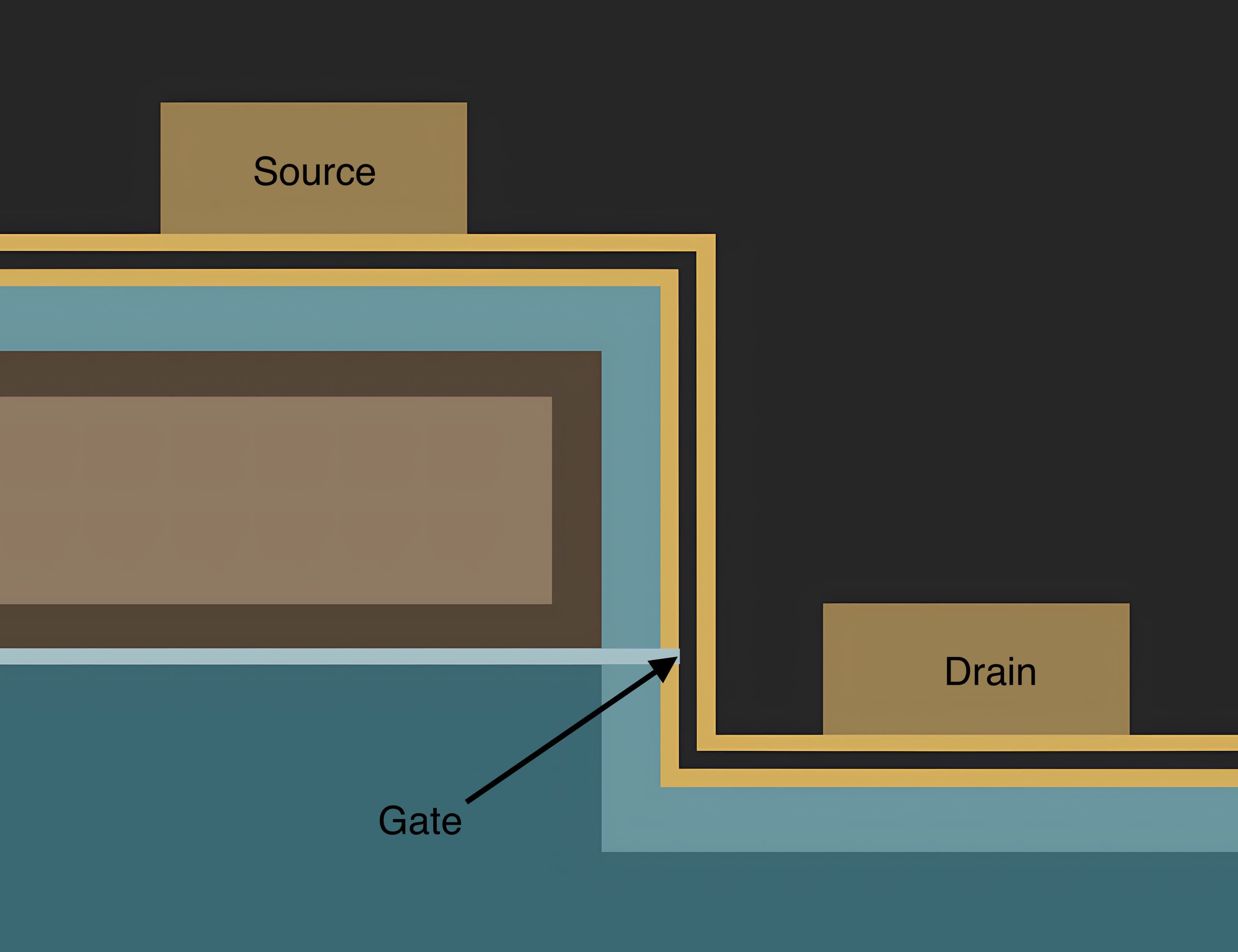
On the upper step, you’ve got the supply, and on prime of the decrease one, you’ve got the drain. Both are fabricated from a titanium palladium alloy separated by the floor of the steps, which is fabricated from a single sheet of a semiconductor materials referred to as molybdenum disulfide, itself resting on a layer of hafnium dioxide that acts as {an electrical} insulator.
The inside of the upper step is a literal sandwich of aluminum coated in aluminum oxide, which rests on prime of a graphene sheet—a single layer of carbon atoms. The aluminum oxide acts as {an electrical} insulator, aside from a small hole within the vertical wall of the upper step, the place the graphene sheet is allowed to contact the molybdenum disulfide. The whole staircase construction rests on a thick layer of silicon dioxide.

The trick to this design is that the sting of the graphene sheet is used, which signifies that when the gate is ready to the “on” state, it is solely 0.34 nm extensive—basically the width of the graphene layer itself. Another notable function of this “side-wall transistor” is its negligible present leakage attributable to larger off-state resistance. Manufacturers may leverage this high quality for low-power purposes. Best of all, it might be comparatively simple to make, though most of the prototypes required fairly a little bit of voltage to drive.
Also learn: ASML’s next-gen EUV machine will give Moore’s Law a brand new lease of life
Tsinghua University researcher Tian-Ling Ren co-authored the research and mentioned this may very well be “the final node for Moore’s legislation.” He additionally believes going smaller than 0.34 nm for the gate dimension is nearly not possible.
Of course, the researchers behind the brand new transistor solely proved {that a} purposeful transistor may very well be made utilizing one-atom skinny supplies with out inventing a brand new course of for precision positioning of the required layers. Reliably constructing billions of those side-wall transistors continues to be a distant dream however is a important step in that route, which fuels hope for quicker, extra power-efficient gadgets sooner or later.
In the meantime, Samsung, Intel, and TSMC are working onerous on making gate-all-around (GAA-FET) transistors a actuality and standardizing interconnects for chiplet designs.
[ad_2]