[ad_1]
In a nutshell: TSMC has simply introduced its whole lineup of 3nm class nodes launching over the following three years. Its new FinFlex tech will give chip designers much more flexibility to optimize every customary cell for the specified energy consumption, efficiency, and density.
TSMC has simply unveiled its whole N3 household of course of nodes. Chip designers equivalent to AMD, Apple, Nvidia, and even Intel will use these nodes over the following few years to manufacture their bleeding-edge chips.
The Taiwanese firm has a complete of 5 totally different 3nm class nodes. N3 will start high-volume manufacturing later this 12 months, with the primary chips anticipated to achieve prospects early subsequent 12 months. N3E will launch later with efficiency and effectivity enhancements, larger yields, however barely lowered logic density.
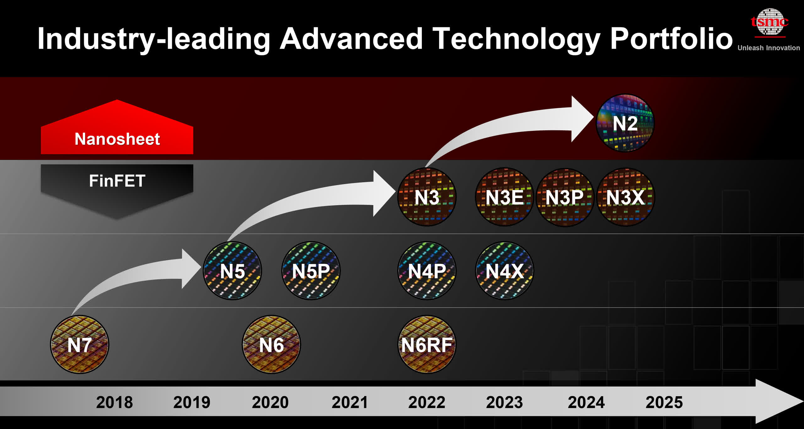
Around 2024, TSMC will deliver out N3P, which focuses on efficiency enhancements. N3S, which wasn’t featured in TSMC’s roadmap, was solely briefly talked about in dialog by SVP Kevin Zhang.
Finally, N3X will come out a couple of 12 months later and permit for very excessive efficiency at larger voltages, with effectivity and prices taking the again seat. This method is just like the 5nm class N4X course of beginning quantity manufacturing subsequent 12 months.
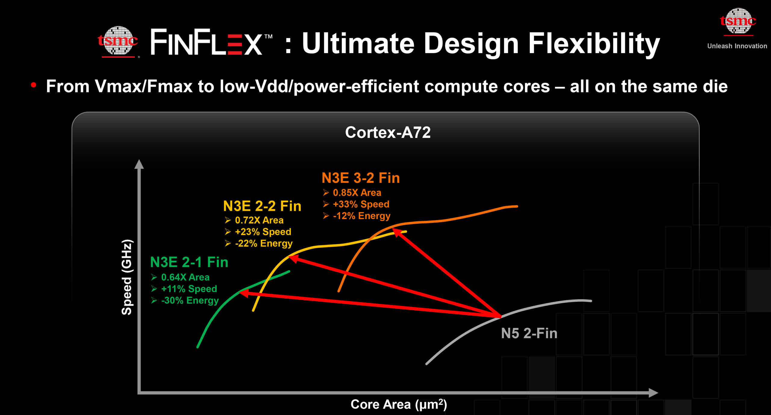
TSMC’s N3 and N3E nodes will even help the corporate’s new FinFlex tech. Currently, chip designers have to choose one library for every block inside an SoC. With FinFlex, they will not have this limitation and can have the ability to combine and match totally different libraries inside every block.
They can use 2-1 (double-gate single-fin) FinFETs in some elements to be able to cut back energy consumption and die measurement (value) and go for 3-2 FinFETs in different areas the place most efficiency is paramount. Meanwhile, 2-2 FinFETs present a stability of measurement, efficiency, and energy consumption.
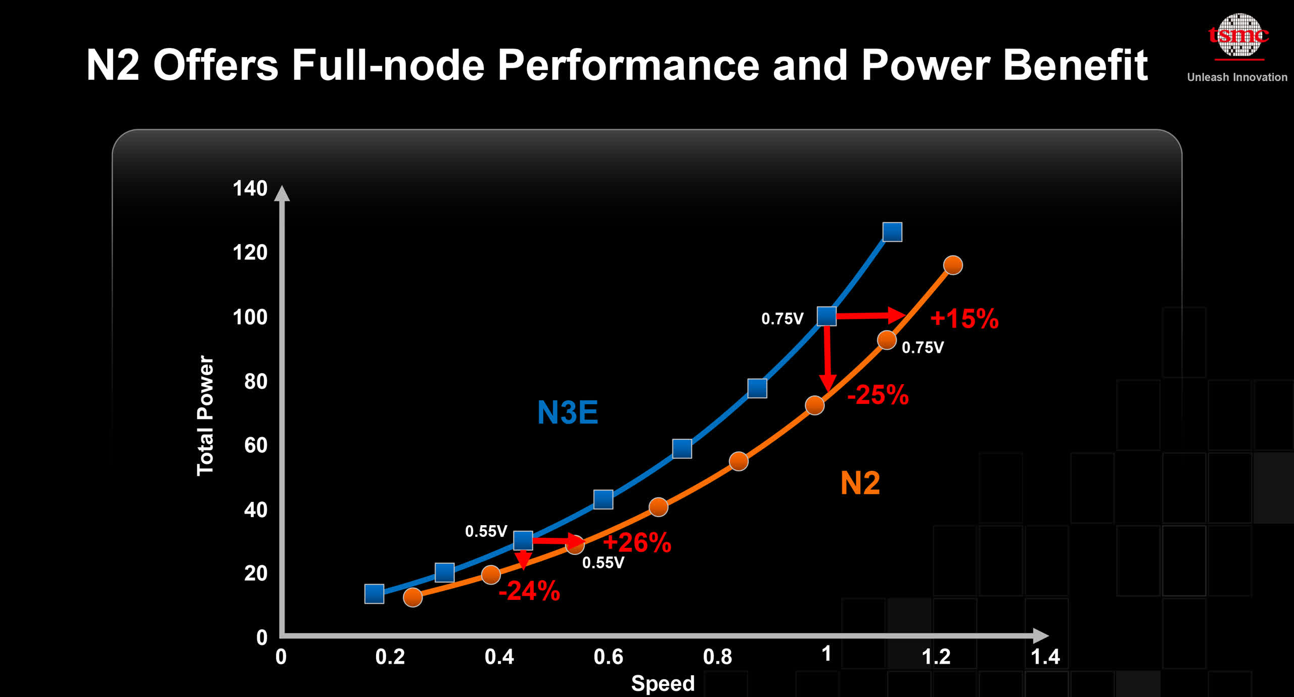
TSMC additionally talked about its upcoming N2 course of node, which can use gate-all-around field-effect transistors (GAAFETs), with plans to start out quantity manufacturing within the second half of 2025.
Compared to N3E, it is going to reportedly draw 25-30 p.c much less energy on the similar frequency and permit for 10-15 p.c extra efficiency with the identical energy consumption and transistor rely. Meanwhile, chip density will reportedly enhance by over 10 p.c.
[ad_2]